
Company news, industry dynamics and technical insight.
Read MST company updates, product releases, industry notes and practical technical articles for MPW, semiconductor equipment design and RFQ preparation.
Browse by column
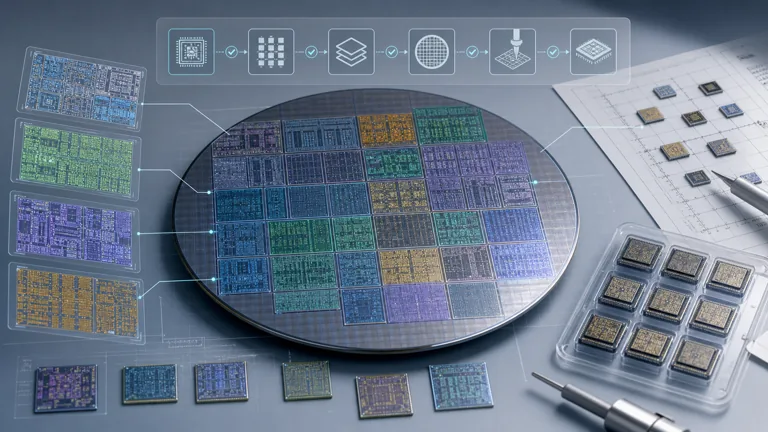
 Company News
MST development and releases
Company updates, service launches, public resources and product release notes from Moore Solution Technology.
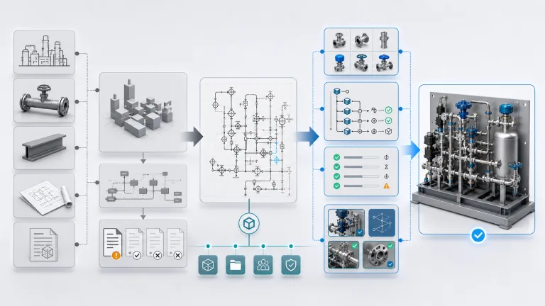
Industry Dynamics
Market and supply-chain notes
Practical notes on mature-node MPW, Asia access, equipment design trends and semiconductor supply-chain changes.
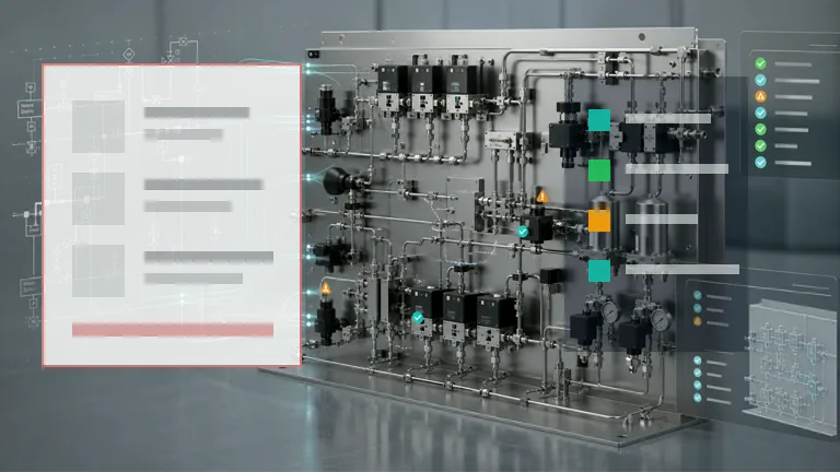
Technical Insights
Engineering guides and explainers
Focused technical articles on MPW flow, PDK/NDA/GDS, package/test, P&ID, BOM context and native SOLIDWORKS assembly.
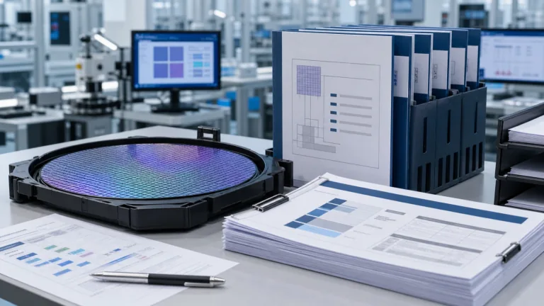
 Product Updates
Tools and service updates
Updates for MST MPW tools, NeuroBox D review workflows and RFQ preparation resources.

From MPW to Engineering Run and Mass Production: What Happens After First Silicon?
First silicon is not the finish line. Learn how MPW results should feed packaging, characterization, engineering run and production planning.
MPW Node Selection: 0.35um, 180nm, 65nm, 40nm and 28nm Tradeoffs
A practical node-selection guide for mature-node MPW scoping across analog, mixed-signal, RF, BCD, high-voltage and digital prototype needs.
MOSIS and Europractice Alternatives: MPW Access Questions for Non-US and Non-Academic Teams
How to think about MPW routes when a team is outside the usual US, European or academic shuttle paths.
Asia MPW Access: What Overseas Fabless Teams Should Prepare
How overseas fabless, university and research teams can prepare a non-confidential MPW access brief before discussing nodes, PDK, NDA, packaging and logistics.
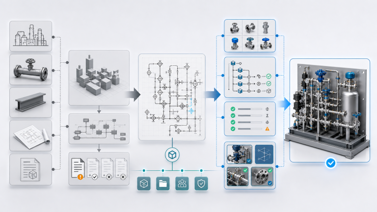
Smap3D Alternative: AI P&ID to Native SOLIDWORKS Assembly
For teams comparing Smap3D alternatives, MST focuses on AI-assisted P&ID-to-native-SOLIDWORKS assembly generation using customer libraries and review exceptions.
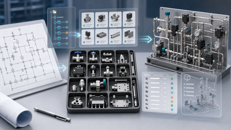
P&ID to 3D Using Your Own SOLIDWORKS Part Library
Why P&ID-to-3D automation should reuse the customer's approved SOLIDWORKS library, BOM fields, naming rules and review standards.
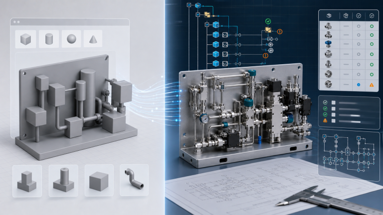
Why AI Text-to-CAD Cannot Produce Production-Oriented SOLIDWORKS Assemblies
AI text-to-CAD can make concept geometry, but P&ID-driven equipment needs native assembly structure, mates, BOM context, part-library reuse and review exceptions.

Sky130 and Open-Source Silicon MPW Options After eFabless
How Sky130, TinyTapeout-style and open-source silicon teams should evaluate MPW route fit, PDK dependency, DRC/LVS status, package and eligibility.
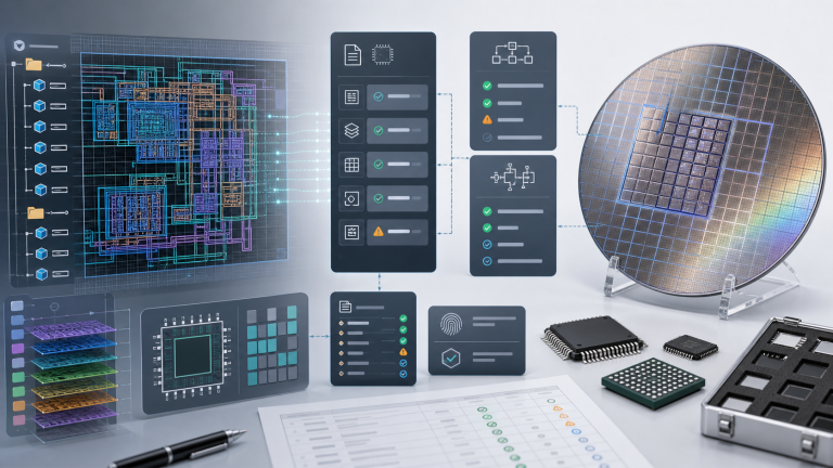
MPW Tapeout Tutorial: Prepare GDSII, DRC and LVS Handoff
Prepare an MPW release package with top-cell identity, DRC/LVS evidence, file checksums and a handoff manifest. Includes a practical walkthrough.
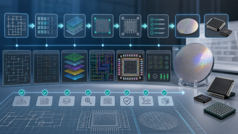
How to Tapeout a Chip: From Final GDS to FAB Out and First Silicon
A practical tapeout guide from process and PDK readiness through final GDS, data acceptance, wafer fabrication, FAB Out, packaging, test and first silicon.
Related tools
MPW RFQ Pack Builder
Turn node, process family, die area, package/test assumptions, timeline and end-use context into a non-confidential first-screen brief.
P&IDP&ID Assembly Intake Checklist
Collect diagram quality, tag index, BOM, part library and rule context before asking whether a native SOLIDWORKS assembly pilot is realistic.
SourcingBOM RFQ Normalizer
Normalize messy BOM rows and expose missing manufacturer, quantity, drawing or description fields before supplier outreach.
Tell us what you need to manufacture, design or source.
Send a short brief for MPW tapeout and manufacturing coordination, a NeuroBox D P&ID-to-native-SOLIDWORKS review, or an engineering procurement RFQ.