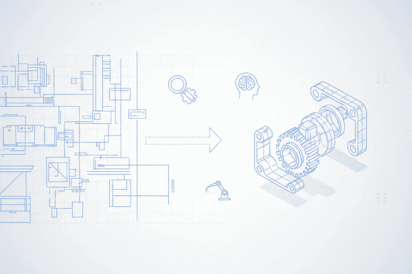
Build vs Buy: Should Your Equipment Company Develop In-House Design Automation?
Key Takeaway Building P&ID-to-SolidWorks automation in-house costs $1.2M+ over two years with no guarantee of production-ready output. The skill intersection…
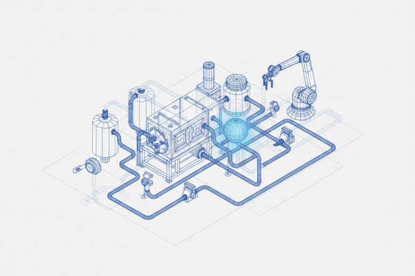
AI Design Automation for Gas Delivery Systems: The Complete Guide
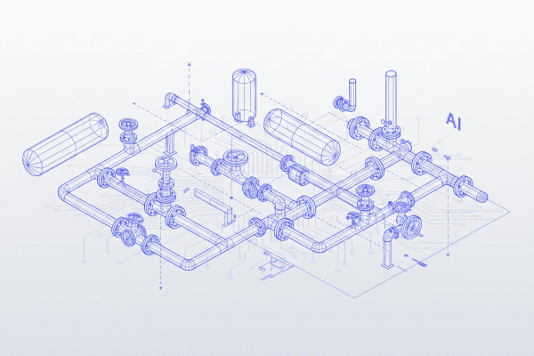
Key Takeaway A typical semiconductor gas panel contains 200+ components with 50+ tube runs that must be routed collision-free in…
NeuroEnergy: AI-Driven Energy Management for Semiconductor Fabs
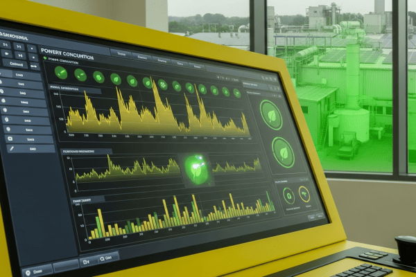
Key Takeaway NeuroEnergy reduces semiconductor fab energy costs by 8-15% through AI-driven optimization. A typical fab consumes 50-100 MW annually…
The Competitive Advantage of Design Speed: Win More Contracts with Faster Equipment Delivery
Key Takeaway In semiconductor equipment procurement, delivery speed has become the primary differentiator after technical qualification. Analysis of 1,840 competitive…
Why Equipment OEMs in Asia Are Adopting AI Design 3x Faster Than Western Competitors
Key Takeaway Equipment OEMs in Asia are adopting AI design automation at roughly 3x the rate of Western competitors, driven…
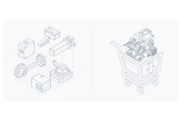
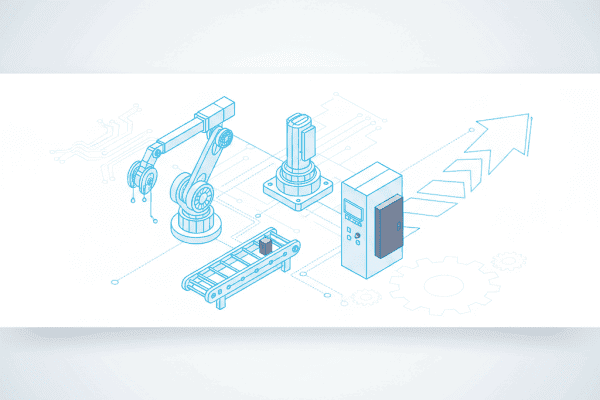
Scaling Equipment Production Without Hiring More Designers: The AI Approach
Key Takeaway Semiconductor equipment demand is projected to grow 8-12% annually through 2030, but the supply of experienced equipment designers…
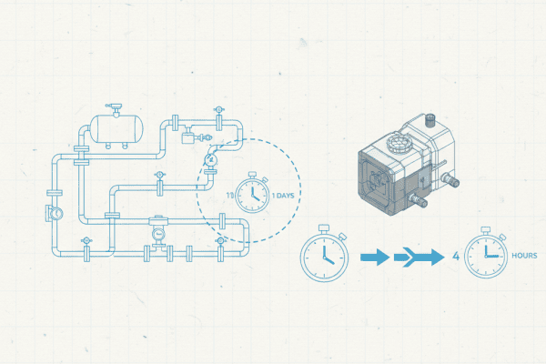
Case Study: How a Gas System Manufacturer Cut Design Time from 10 Days to 4 Hours
Key Takeaway A specialty gas system manufacturer reduced their standard gas panel design cycle from 10 working days to 4…
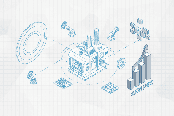
ROI Calculator: What AI Design Automation Saves Your Equipment Company Per Year
Key Takeaway For a mid-sized semiconductor equipment OEM (40-60 projects/year, $80-150M revenue), AI design automation delivers $1.8-4.2M in annual savings…
AI-Assisted Design Review: Catching Errors Before They Reach the Shop Floor
Key Takeaway Traditional design review catches 78-85% of errors but consumes 15-22% of total project engineering time. AI-assisted design review…
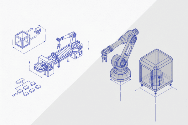
Automated Piping and Tubing Layout: How AI Solves the 3D Routing Problem in Equipment Design
Key Takeaway 3D piping and tubing routing is the most time-consuming phase of semiconductor equipment design, consuming 40-55% of total…
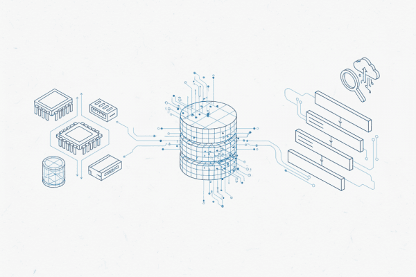
From Component Library to Intelligent Parts Database: AI-Powered BOM Management
Key Takeaway Traditional component libraries store geometry. Intelligent parts databases store engineering knowledge: application constraints, compatibility rules, procurement data, and…
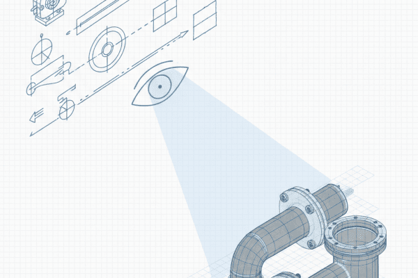
How AI Reads P&ID Symbols: Computer Vision for Engineering Diagrams Explained
Key Takeaway Modern computer vision systems can parse P and ID diagrams with 97-99% symbol recognition accuracy and 94-96% connectivity…