Computing Cpk for Multi-Chamber Tools: Three Correct Approaches and Variance Decomposition in Practice
Single-chamber Cpk 1.67 dropping to pooled 1.20 is not a process problem — it is matching variance showing up in…

HBM4 and Chiplet Yield Bottleneck: Why FDC Matters More Than VM in Advanced Packaging
HBM4 16-layer stacking plus CoWoS-L integration shifts yield from per-die to per-package. This article breaks down the chiplet yield math,…

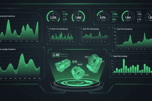
In-Chamber Visual AI: A Roadmap for Equipment OEMs to Ship Smart Tools
Semiconductor visual AI is shifting from fab-side defect classification to equipment-side real-time sensing. This article breaks down three technical paths…
Why Your Virtual Metrology Model Isn’t Accurate — And How to Fix It
5 common pitfalls that degrade VM accuracy in production: training data bias, missing features, post-PM drift, chamber variation, sensor decay.…
AI vs Traditional SPC in Semiconductor Manufacturing: A 2026 Comparison
Key Takeaway AI-driven process control (Virtual Metrology + Run-to-Run) detects process drift 10–50× faster than traditional SPC and improves yield…
OCAP Explained: The Complete Out-of-Control Action Plan for Semiconductor Fabs
Key Takeaway: OCAP (Out of Control Action Plan) is the standardized procedure semiconductor fabs follow when SPC charts detect an…
Process Window Optimization: How AI Finds the Sweet Spot for Maximum Yield
Key Takeaway: A process window defines the safe operating range where semiconductor processes produce acceptable yield. AI-powered response surface modeling…
Real-Time Flow Interruption Detection in CVD Equipment: How AI Catches What Engineers Miss
Flow interruption in CVD equipment causes batch yield loss but goes undetected until post-process metrology. NeuroBox E5200V deploys real-time video…
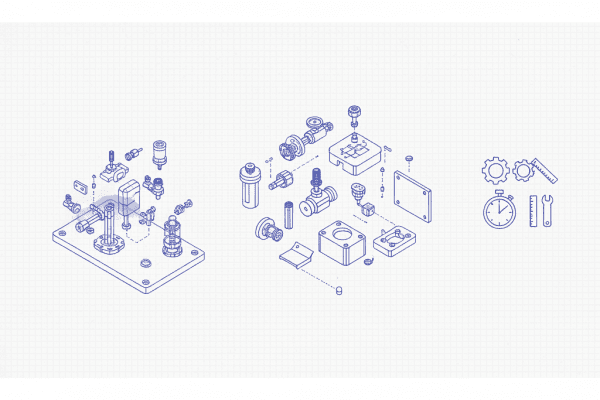
How Many SolidWorks Hours Does Your Gas Panel Really Need? Industry Benchmarks
Key Takeaway A typical semiconductor gas panel requires 320-480 SolidWorks person-hours for mechanical design, with routing and interference resolution consuming…

AI for Wafer Inspection: From Manual Classification to Automated Defect Recognition
Key Takeaway Wafer defect inspection generates terabytes of image data daily, yet 30-50% of detected defects are nuisance defects that…