- →1. Why advanced packaging yield logic has changed
- →2. Why VM is insufficient for advanced packaging
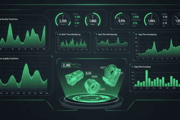
- →3. FDC becomes the #1 AI weapon in advanced packaging
- →4. From single-tool FDC to package-level FDC
- →5. Six essentials for deploying advanced-packaging FDC
Key Takeaways
Entering the HBM4 and CoWoS-L era, the advanced packaging yield bottleneck has shifted from “single die” to “chiplet integration.” A 16-layer HBM4 stack combined with 2.5D/3D integration means any single bad die or failed bonding step scraps the entire package. The math is brutal: 16 layers with 99.5% per-layer yield gives ~92% overall; at 99% per layer, that falls to 85%. This makes FDC (fault detection) more critical than VM (virtual metrology) in advanced packaging — because bonding anomalies must abort the recipe in real time, not wait for post-process measurement. This article breaks down chiplet yield math and six deployment essentials for advanced-packaging FDC.
1. Why advanced packaging yield logic has changed
Traditional fab yield logic is “maximize good die per wafer” — the die is the smallest yield unit, and losing a die is a linear loss.
In the 2.5D/3D advanced packaging era, that logic flips: the die is no longer the smallest yield unit — the package is. Pair a HBM4 stack with a GPU logic die, integrate via CoWoS-L, and any bad die or failed bonding step scraps the entire package (USD 10,000–30,000 of value).
The raw math:
| Integration level | 99.0% per layer | 99.5% per layer | 99.9% per layer |
|---|---|---|---|
| HBM3 (8 layers) | 92.3% | 96.1% | 99.2% |
| HBM3E (12 layers) | 88.6% | 94.2% | 98.8% |
| HBM4 (16 layers) | 85.1% | 92.3% | 98.4% |
| HBM4 + GPU + CoWoS-L | ~75–80% | ~88–90% | ~96–97% |
The last row is what matters. Composite HBM4 + GPU package yield is extraordinarily sensitive to per-layer yield. Improving from 99% to 99.5% isn’t “slightly better” — it’s the difference between commercial viability and a dead product.
2. Why VM is insufficient for advanced packaging
Virtual Metrology (VM) is one of the most mature semiconductor AI applications — using chamber sensor data to predict wafer thickness, uniformity, and critical dimensions. VM works well in front-end processes because “after the fact” still leaves room to adjust the next lot (e.g., detect CD drift and tune litho on the next batch).
In bonding, VM’s “after the fact” philosophy breaks:
Challenge 1: Bonding is irreversible. Once two dies are joined via Cu-Cu hybrid bonding, atomic-level diffusion has happened. Even if VM detects a bonding quality issue, there’s no redo — the whole package is scrap.
Challenge 2: The downstream test window is too narrow. HBM KGD (Known Good Die) testing happens after stack completion, when defects have already accumulated to the final unit. Unlike front-end lots, there’s no “re-probe after electrical test and rework.”
Challenge 3: Package-level value density is too high. An HBM4 stack costs USD 800–1500 to produce; a GPU logic die costs USD 3,000–5,000. A fully CoWoS-integrated package exceeds USD 10,000. VM’s “reduce yield loss” philosophy isn’t aggressive enough at this value density — what’s needed is “real-time abort.”
3. FDC becomes the #1 AI weapon in advanced packaging
Fault Detection and Classification (FDC) was traditionally treated as a process monitoring tool, peer-ranked with VM in front-end etch/CVD. In advanced packaging, FDC becomes more urgent than after-the-fact VM because it can support real-time abort or hold decisions during bonding when the tool, recipe, and factory control path are validated for that response.
Three critical FDC capabilities for advanced packaging:
Capability 1: Real-time anomaly detection on bonding temperature and pressure
Cu-Cu hybrid bonding requires precise temperature (typically 250–400°C) and pressure (5–50 MPa) profiles. A 0.5-second thermal overshoot or 1% pressure deviation can cause voids or incomplete bonding. FDC must detect these in milliseconds and trigger recipe abort — classical SPC cannot do this.
Capability 2: TCB (Thermal Compression Bonding) force profile monitoring
Modern TCB tools capture thousands of time-series data points per bonding event (force, temperature, z-axis position). FDC models learn the multi-dimensional time-series patterns of “normal bonding”; any deviation beyond threshold triggers alerts. Rule-based approaches cannot handle this high-dimensional pattern recognition.
Capability 3: Underfill flow anomaly detection
Underfill flowability between chiplets directly affects thermal performance and mechanical reliability. Voids or incomplete fills are invisible to simple optical inspection — FDC combines dispense flow rate, temperature profile, and acoustic signals in multi-modal fusion to judge underfill quality in real time.
4. From single-tool FDC to package-level FDC
Single-tool FDC is now industry standard (Besi and ASMPT TCB tools ship with basic FDC). But advanced packaging yield problems truly require cross-tool, cross-layer FDC correlation:
A HBM4 stack goes through 16 bonding operations, multiple underfill dispenses, and several KGD tests. Each step’s FDC data, viewed alone, may look “normal.” But a joint analysis across 16 layers might reveal that layer 5’s bonding temperature is consistently slightly low, and the KGD failure rate between layers 5 and 6 is 3× other layers — a pattern only visible at package-level FDC.
This is why single-tool FDC is insufficient. Fabs need a platform that spans all bonding tools, collects from them, and runs joint analysis.
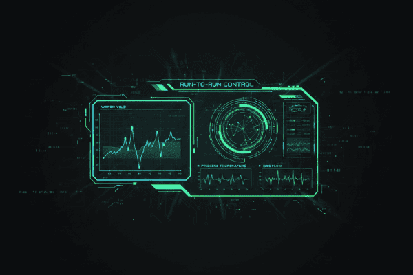
5. Six essentials for deploying advanced-packaging FDC
1. Minimum 100Hz sampling rate. Critical anomalies in HBM bonding occur at sub-second timescales. Classical SECS/GEM 1Hz is far too slow; upgrade to 10ms intervals.
2. Multi-modal data fusion. Temperature and pressure alone aren’t enough — add AE (acoustic emission), dispense flow rate, and die-to-die alignment camera. Best-in-class packaging fab FDC systems integrate 20+ sensor modalities.
3. Models must be stack-aware. Layer 1 and layer 16 have different “normal” temperature profiles (heat accumulation, thermal mass changes above). FDC models must know the current layer index and use the right baseline.
4. Tiered abort authority. Not every anomaly should halt the line — distinguish “scrap this package” vs. “halt this tool” vs. “adjust next package parameters.” Requires deep FDC–MES/EDA integration.
5. Reserve data recirculation. Every aborted full profile must flow back to model training pipelines. Advanced packaging evolves fast (HBM3 → 3E → 4 in three years); models need continuous refresh.
6. Closed loop with KGD test results. Failed KGD packages must be traceable back to each layer’s FDC profile — that’s how you keep refining “anomaly definitions.” Many fabs skip this closure, leaving FDC stuck at “looks useful.”
6. MST NeuroBox’s role in advanced-packaging FDC
MST NeuroBox E3200 is primarily positioned for front-end etch/CVD VM/R2R/FDC, but the core architecture extends to advanced packaging. Three collaboration directions with packaging OEMs:
1. Bonding tool FDC modules — proposed as an OEM factory option (on the roadmap; not yet available), designed to add 100Hz sampling + multi-modal FDC to TCB / hybrid bonding tools.
2. Package-level FDC aggregation platform — designed to be deployed fab-side (concept/roadmap; not yet deployed), integrating multiple bonding tools and KGD testers for cross-tool FDC correlation.
3. HBM-specific FDC model library — an intended approach to pre-train on partner data (no partner or customer data exists yet; contingent on future partner collaboration) for HBM bonding / underfill anomaly recognition, after which customer fabs would need only small fine-tuning.
7. Strategic implications for HBM and CoWoS supply chains
A strategic note: in 2026, global HBM demand far exceeds supply, and the primary bottleneck isn’t wafer capacity — it’s advanced packaging yield. A company that lifts HBM4 yield from 85% to 92% effectively adds 8% of capacity. In a market where HBM exceeds USD 1,000/GB, that’s billions of dollars of value.
This is why TSMC, Samsung, and SK Hynix all launched AI-driven packaging yield programs in 2025–2026. Packaging-side FDC + AI is no longer a “nice to have” — it directly determines competitive position.
If you work on process or yield in HBM / CoWoS / chiplet-related business, NeuroBox E3200‘s FDC platform supports advanced packaging extensions. Book a 45-minute technical review focused on advanced-packaging FDC.
Related reading
Scope a SECS/GEM equipment integration request
Share the equipment model, physical interface, current protocol and target host. Start with a non-confidential outline; detailed files can follow through the controlled review path.
Check integration fit →