All
19
AI Business Strategy
AI Process Control
Company News
Design Automation
Energy Management
Equipment Communication
Equipment Operations
equipment-operations
Industry Trends
Product News
Semiconductor Process
Smart DOE
Uncategorized
Process-Specific AI: Why One-Size-Fits-All Doesn’t Work for Etch, CVD, CMP, and Litho
Generic AI fails because each semiconductor process has different data, dynamics, and objectives. Practical comparison across etch, CVD, CMP, and…
The Complete Guide to Semiconductor Wafer Manufacturing: From Silicon to Finished Chip
A comprehensive walkthrough of the entire wafer manufacturing journey — from crystal growth to final test — with insights on…

AI for Wafer Inspection: From Manual Classification to Automated Defect Recognition
Key Takeaway Wafer defect inspection generates terabytes of image data daily, yet 30-50% of detected defects are nuisance defects that…

AI for Wet Cleaning Equipment: Chemical Concentration Monitoring and Defect Prevention
Key Takeaway Wet cleaning accounts for 15-20% of all process steps in semiconductor manufacturing, yet chemical bath monitoring still relies…
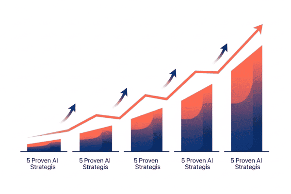
Semiconductor Yield Improvement: 5 Proven AI Strategies That Work
Key Takeaway Yield improvement remains the highest-leverage activity in semiconductor manufacturing, where a 1% yield gain at an advanced node…