
会社ニュース、業界動向、技術インサイト。
MST の会社アップデート、製品リリース、業界ノート、MPW、半導体装置設計、RFQ 準備に関する実務的な技術記事を掲載します。
カテゴリー別に見る
 会社ニュース
MST の展開とリリース
Moore Solution Technology の会社アップデート、サービス開始、公開リソース、製品リリース情報。
業界動向
市場とサプライチェーンのノート
成熟ノード MPW、アジアでのアクセス、装置設計トレンド、半導体サプライチェーン変化に関する実務的な解説。
技術インサイト
エンジニアリングガイドと解説
MPW フロー、PDK/NDA/GDS、package/test、P&ID、BOM context、ネイティブ SOLIDWORKS assembly に関する技術記事。
 製品アップデート
ツールとサービスの更新
MST MPW tools、NeuroBox D review workflow、RFQ 準備リソースの更新情報。
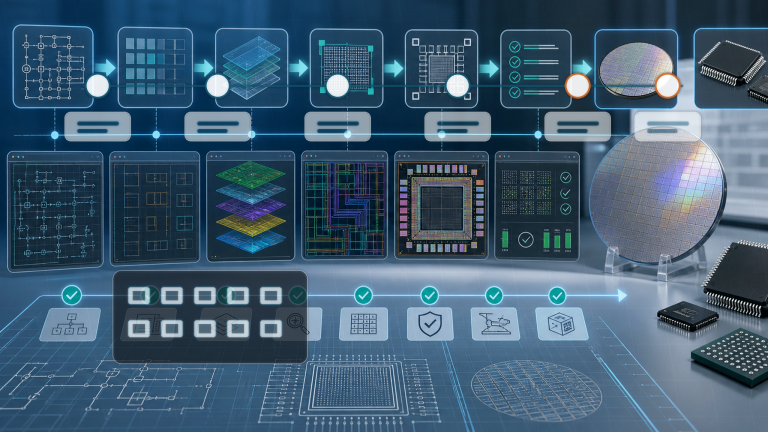
MPW から engineering run と量産へ: 初回シリコン後の流れ
First silicon is not the finish line. Learn how MPW results should feed packaging, characterization, engineering run and production planning.
MPW ノード選定: 0.35um、180nm、65nm、40nm、28nm の比較
A practical node-selection guide for mature-node MPW scoping across analog, mixed-signal, RF, BCD, high-voltage and digital prototype needs.
米欧圏外チーム向け MOSIS / Europractice 代替ルート
How to think about MPW routes when a team is outside the usual US, European or academic shuttle paths.
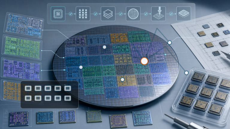
シンガポールとアジアの MPW アクセス: 海外チームの準備事項
How overseas fabless, university and research teams can prepare a non-confidential MPW access brief before discussing nodes, PDK, NDA, packaging and logistics.
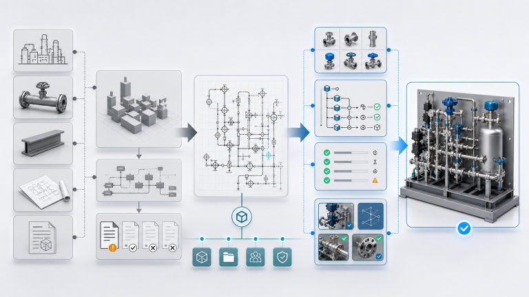
Smap3D 代替: P&ID からネイティブ SOLIDWORKS アセンブリへ
For teams comparing Smap3D alternatives, MST focuses on AI-assisted P&ID-to-native-SOLIDWORKS assembly generation using customer libraries and review exceptions.
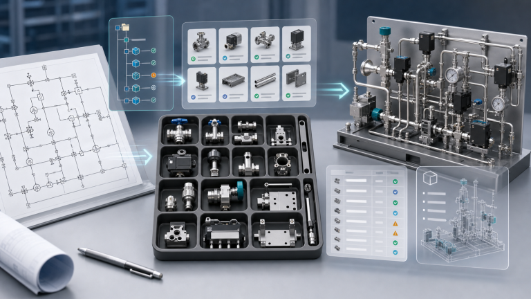
P&ID to 3D Using Your Own SOLIDWORKS Part Library
Why P&ID-to-3D automation should reuse the customer's approved SOLIDWORKS library, BOM fields, naming rules and review standards.
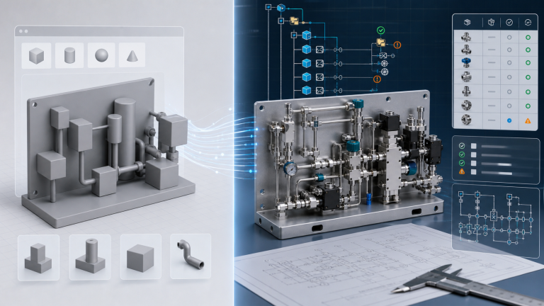
Why AI Text-to-CAD Cannot Produce Production-Oriented SOLIDWORKS Assemblies
AI text-to-CAD can make concept geometry, but P&ID-driven equipment needs native assembly structure, mates, BOM context, part-library reuse and review exceptions.
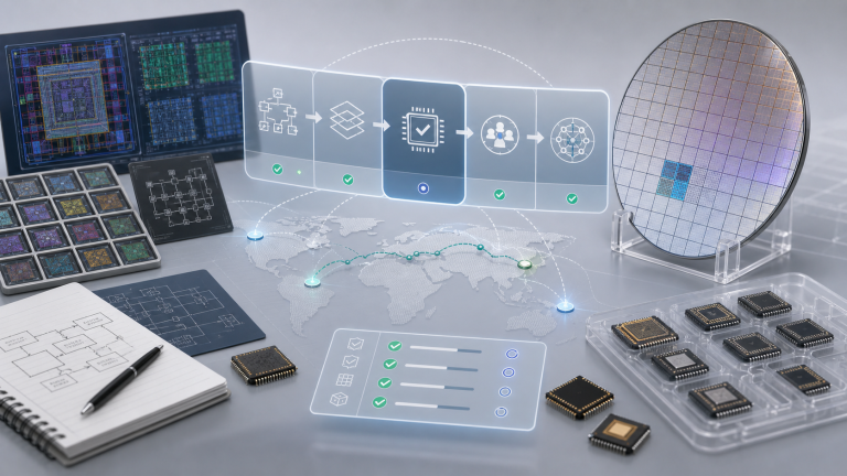
eFabless 後の Sky130 とオープンソース MPW の選択肢
How Sky130, TinyTapeout-style and open-source silicon teams should evaluate MPW route fit, PDK dependency, DRC/LVS status, package and eligibility.
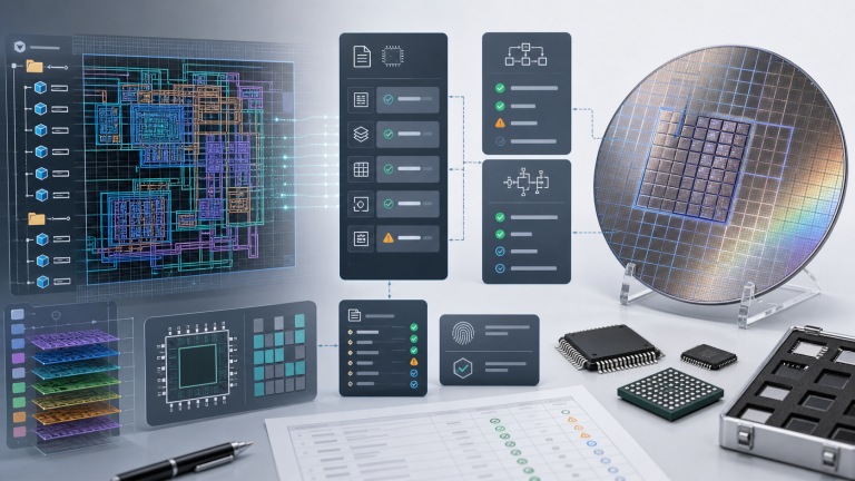
MPW tapeout に必要な GDSII、DRC、LVS
Prepare an MPW release package with top-cell identity, DRC/LVS evidence, file checksums and a handoff manifest. Includes a practical walkthrough.
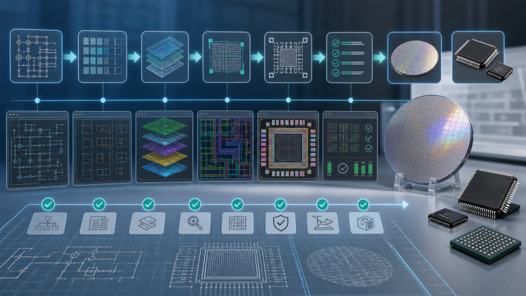
チップ tapeout の進め方: 初回シリコンのチェックリスト
A practical tapeout guide from process and PDK readiness through final GDS, data acceptance, wafer fabrication, FAB Out, packaging, test and first silicon.
Related tools
MPW RFQパックビルダー
Turn node, process family, die area, package/test assumptions, timeline and end-use context into a non-confidential first-screen brief.
P&IDP&ID Assembly Intake Checklist
Collect diagram quality, tag index, BOM, part library and rule context before asking whether a native SOLIDWORKS assembly pilot is realistic.
調達BOM RFQ正規化ツール
Normalize messy BOM rows and expose missing manufacturer, quantity, drawing or description fields before supplier outreach.
製造・設計・調達したい内容をお知らせください。
MPW tapeout と製造調整、NeuroBox D P&ID-to-3D review、または engineering procurement RFQ について短い brief を送ってください。