Multi-Project Wafer (MPW) Shuttle: Complete Guide for First Silicon
A complete MPW shuttle guide for first silicon: what MPW means, who uses it, what affects cost and schedule, and what to prepare before RFQ.
- →What is an MPW shuttle?
- →Who uses MPW?
- →What information is needed before an MPW RFQ?
- →MPW vs full mask
- →Where MST fits
Answer block: A multi-project wafer, or MPW shuttle, lets multiple chip projects share mask or wafer resources so teams can obtain prototype silicon before committing to a dedicated full-mask route. MPW is useful for first silicon, IP validation, analog/RF/power experiments, university research and startup prototyping. MST coordinates mature-node MPW RFQs as a screening and routing partner, not as a wafer foundry.
Many engineers search for MPW only after they already need an RFQ. That misses the bigger planning question: what has to be ready before a chip can be put on a shuttle? This guide is the hub for MST’s MPW content: what MPW means, how a first tapeout works, what affects cost and timeline, and when a team should move from MPW to full mask.
What is an MPW shuttle?
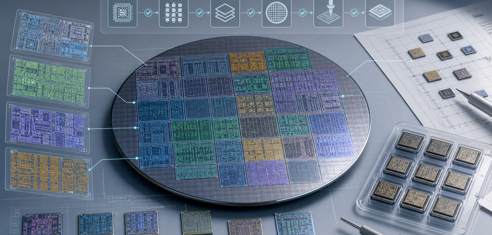
An MPW shuttle is a shared tapeout route. Instead of one design owner paying for a dedicated mask set and wafer run, multiple projects are grouped into a shared shuttle window. Public examples of shared shuttle programs include foundry shuttle services such as TSMC CyberShuttle, academic or research access programs such as Europractice, and broader access organizations such as MOSIS.
The important point is not the name of the program. The important point is fit: node, process family, design rules, PDK access, package, test expectations, export-control constraints, schedule and commercial eligibility.
Who uses MPW?
- Fabless startups use MPW to obtain first silicon before a full commercial mask commitment.
- IC design teams use it to validate IP blocks, analog front ends, sensor interfaces, RF circuits or power-management designs.
- Universities and research labs use MPW for teaching, papers, prototypes and open-source silicon experiments.
- Industrial buyers use MPW planning to compare prototype routes, package options and test responsibilities.
What information is needed before an MPW RFQ?
A first MPW conversation should not include GDS, netlist, RTL or private design IP. Start with non-confidential requirements:
- Target node or approximate node range.
- Process family: CMOS logic, analog/mixed-signal, RF, BCD, high-voltage, sensor, eNVM or MEMS-related needs.
- Approximate die area and expected sample quantity.
- PDK status and whether NDA access is already available.
- Package, wafer probe, test and logistics expectations.
- Country, company type, end-use context and target schedule.
For a practical intake checklist, see What Information Is Needed for an MPW RFQ? and Can You Start an MPW RFQ Without GDS?.
MPW vs full mask
MPW is usually the first-silicon and validation route. Full mask is usually the route for stronger schedule control, volume planning and dedicated production work. The tradeoff is not simply price. Teams compare schedule, die area, process maturity, partner eligibility, packaging, expected spins and how much control they need over the run.
| Question | MPW shuttle | Full mask |
|---|---|---|
| Best for | Prototype silicon and validation | Dedicated program control |
| Schedule | Depends on shuttle windows | Planned around the dedicated route |
| Cost structure | Shared resources | Dedicated mask and wafer economics |
| Design readiness | Still requires signoff discipline | Requires stronger release control |
For a deeper comparison, read MPW vs Full Mask: Which Tapeout Route Should You Choose?.
Where MST fits
MST is not a wafer foundry and does not claim to manufacture wafers directly. MST’s role is MPW aggregation and RFQ coordination: screening high-level requirements, checking process fit, preparing the non-confidential brief, coordinating NDA/PDK path where applicable, and routing qualified RFQs to suitable partner routes.
FAQ
Is MPW the cheapest way to prototype a chip?
It can be a practical prototype route because resources are shared, but the final economics depend on node, die area, shuttle access, package, test and commercial eligibility.
Can I start without GDS?
Yes. For first screening, start with high-level requirements only. Do not send GDS or design IP at intake.
Does MPW include packaging and test?
Not automatically. Packaging, wafer probe, sample count and test expectations should be specified early so the route can be scoped correctly.
Start with the MST mature-node MPW hub or use the open MPW planning tools before submitting an RFQ.
Related Articles

Ready to plan your MPW and first-silicon path?
Start with a non-confidential brief covering node/process fit, schedule, first-silicon validation, packaging/test, sample handling or re-spin needs. MST routes the request for review; feasibility, availability, timing and quotation are confirmed case by case.