
MPW vs Pilot Wafer vs Full Mask: Which Route Fits Your Chip?
A practical decision guide to shared MPW, pilot wafer or engineering lots, and dedicated full-mask production—covering maturity, schedule, splits, samples, package, test and scale-up.
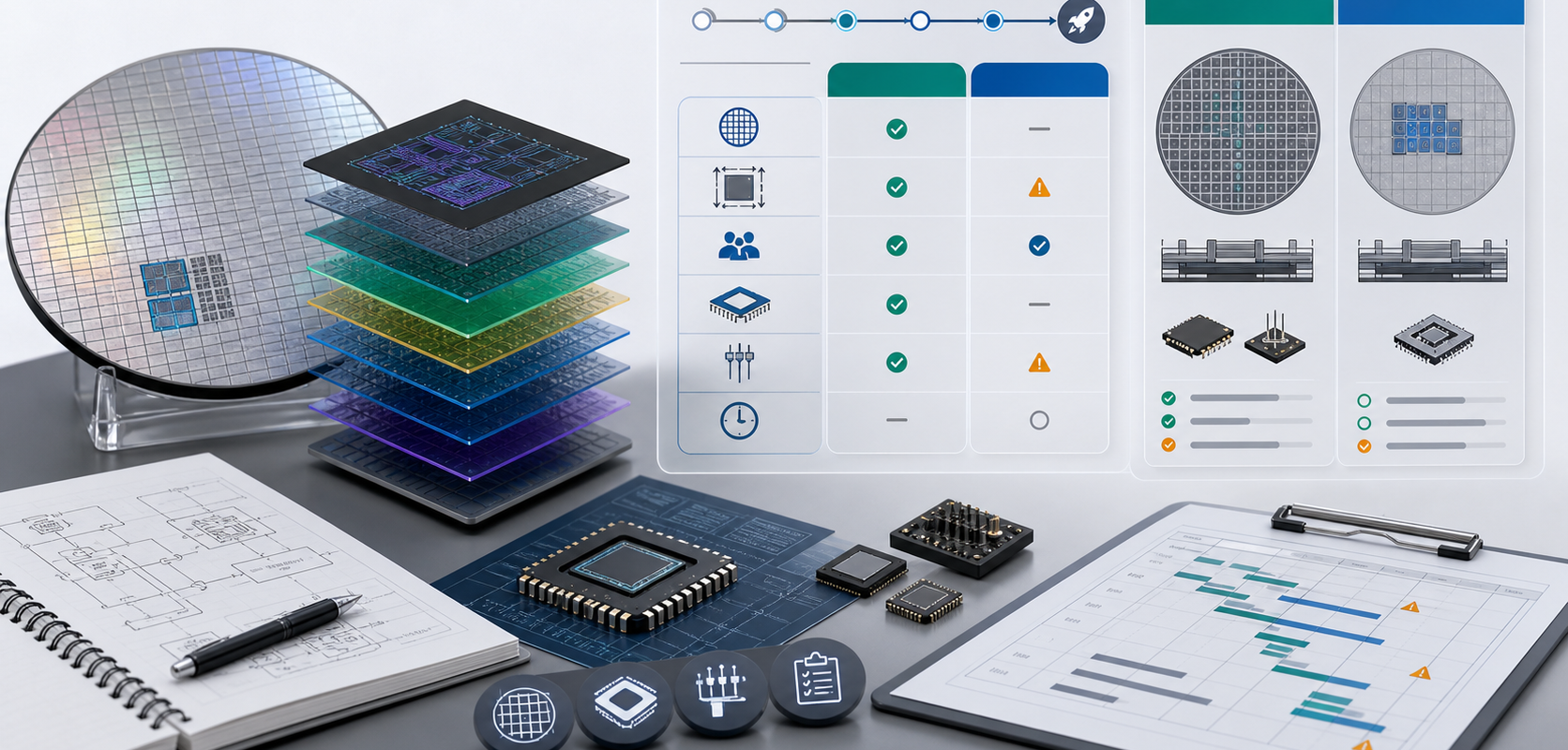
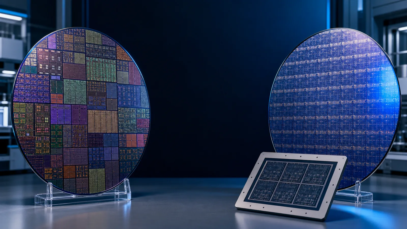
MPW, pilot wafer and full mask answer different questions
Many comparison articles place MPW, pilot wafer and full mask in one row as if they were three standardized products. That shortcut is useful for a first explanation, but it can create an expensive misunderstanding during an RFQ.
- MPW describes a sharing model. Multiple projects share mask and wafer resources under a scheduled program. The immediate objective is usually prototype silicon, design learning or a limited sample need.
- Pilot wafer or engineering lot describes a development stage and lot purpose. It commonly means a small, more controlled wafer run used after a design has reached a higher maturity level. The provider may use a dedicated mask set, a multi-level-mask strategy or another engineering arrangement.
- Full mask describes the mask strategy. A customer funds a dedicated mask set rather than sharing it with other projects. That mask set may support an engineering lot, qualification lots or production wafer starts, depending on the commercial and manufacturing agreement.
This distinction matters because a buyer can request a dedicated mask but still be ordering an engineering lot, not volume production. Conversely, a provider may offer a prototype route that is more flexible than MPW without calling it “pilot wafer.” X-FAB, for example, publicly distinguishes scheduled MPW, multi-level-mask prototyping and standard engineering lots. GlobalFoundries’ partner overview distinguishes MPW, dedicated masksets and production lots. The vocabulary must therefore be translated into a written scope, not assumed from a label.
| Decision | MPW / shared shuttle | Pilot wafer / engineering lot | Dedicated full-mask production route |
|---|---|---|---|
| Primary purpose | Obtain first silicon and learn | Characterize, split, qualify or prepare customer samples | Ramp a stable design under a production plan |
| Mask model | Shared across projects | Provider-specific; often dedicated, but must be confirmed | Dedicated mask set |
| Schedule control | Bound to available shuttle windows and data deadlines | More project-specific, subject to engineering capacity and scope | Planned against qualified capacity, forecast and wafer demand |
| Typical output question | “Does the design work in silicon?” | “Is performance stable enough across the agreed test and process plan?” | “Can the product be manufactured, tested and supplied at the required scale?” |
| Commercial behavior | Shared early access; limited area and sample rules | Higher project-specific NRE and wafer commitment | Highest upfront mask commitment, then production economics matter |
| Best fit | Design risk remains and a re-spin is plausible | Silicon evidence exists, but characterization or qualification evidence is incomplete | Design, demand, package and test plan are stable enough to ramp |
A practical route-selection test
The right route is determined by the next evidence your business needs, not by which option sounds more advanced.
| Gate | If the answer is “no” | If the answer is “yes” |
|---|---|---|
| Do you already have measured silicon from this design revision? | Start by screening an MPW or other prototype route. | Move to the next gate. |
| Are the main functional, analog, RF, memory or power targets demonstrated? | A re-spin or another prototype may be safer than a dedicated lot. | Move to characterization and manufacturing questions. |
| Are package, probe, final test and bring-up methods defined? | Close the post-fab plan before committing more wafers. | Evaluate a pilot or engineering lot. |
| Are the requested process splits, stress conditions and acceptance limits written? | Do not assume a pilot lot automatically includes them. | Ask the provider to quote the exact engineering plan. |
| Is there a credible volume forecast and qualified supply-chain plan? | Stay in engineering or limited-volume planning. | Evaluate dedicated mask and production wafer starts. |
A first-time team often moves through MPW → first-silicon bring-up → ECO/re-spin decision → engineering lot or pilot build → qualification and customer sampling → production. This is a useful planning sequence, not a universal contract. Some products need more than one MPW; some move directly from a successful prototype to a dedicated engineering run; some specialty processes use different prototype structures entirely.
Pilot wafer is not a universal product name
“Pilot wafer” may refer to a small dedicated wafer lot, a risk-production step, an engineering lot, a qualification precursor or a pilot-line process-development run. Those meanings are not identical. An RFQ should replace the shorthand with explicit deliverables.
In particular, a pilot or engineering lot does not automatically include process-corner splits. Digital library labels such as slow, typical and fast describe characterized model corners; they are not a promise that a buyer receives separate wafer lots for every named corner. Process splits, voltage and temperature characterization, PCM targets, wafer quantities, sampling plans and qualification conditions must be written into the provider-approved plan.
| Question to put in the RFQ | Why it matters |
|---|---|
| Is the mask set shared, multi-level or fully dedicated? | “Pilot” alone does not define mask ownership or reuse. |
| How many wafer starts, completed wafers and shipped wafers are included? | Starts, completions and deliverables may differ after process disposition. |
| Which process splits or module options are included? | Extra splits can change schedule, wafer count and price. |
| What PCM, wafer-sort or final-test data will be delivered? | “Wafers delivered” does not define the evidence package. |
| Are probe, backgrind, dicing, packaging and final test included? | FAB Out normally does not mean finished, tested packaged parts. |
| What are the hold points, ECO rules and mask-revision charges? | Engineering flexibility must be agreed before data release. |
| What is the acceptance criterion for moving toward production? | A pilot lot should close defined risks, not merely create more samples. |
What actually changes inside the manufacturing path
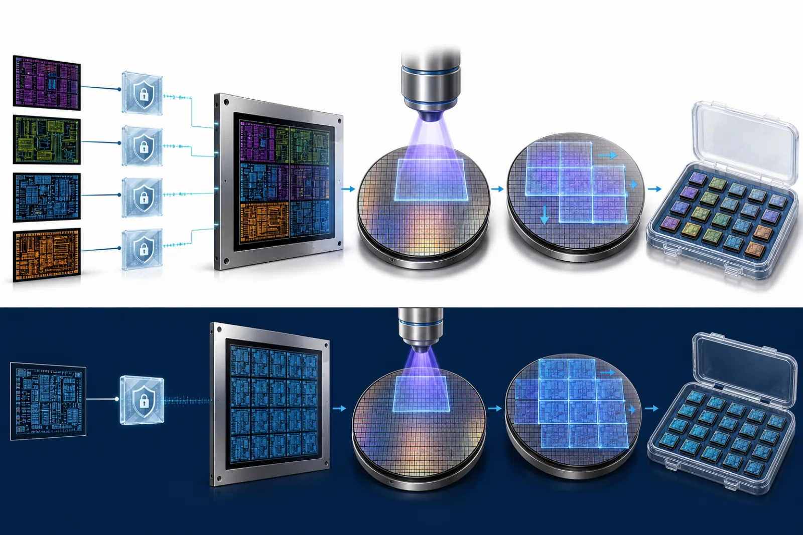
After customer data acceptance, the manufacturing data path may include layout preparation, optical-proximity correction where required, mask-data preparation, fracturing, mask verification and mask writing before wafer lithography. Synopsys’ public mask-synthesis material documents the GDSII/OASIS, OPC, fracturing and mask-writer handoff stages. The exact data owner and sign-off responsibilities vary by foundry and node.
In an MPW program, multiple customer projects are aggregated under the program’s reticle and wafer plan. Samsung Foundry describes MPW as placing multiple designs on one wafer so customers can share masks; GlobalFoundries similarly describes multiple projects aggregated onto a wafer. The shuttle operator or foundry controls the accepted floorplan and manufacturing release. A customer should not assume that a diagram in a marketing article represents the actual reticle layout.
In a dedicated route, one customer design owns the relevant mask strategy and wafer plan. That creates more control, but it also moves more mask, wafer, test and disposition risk to that program.
Three common reticle myths
- “Every MPW uses a fixed 2 × 2 mm seat.” It does not. Block size, minimum area and reticle rules vary by program. Some services sell standard blocks, some use minimum areas, and some quote a custom accepted footprint.
- “The customer can freely pack the shared reticle.” Usually the service provider owns aggregation, compatibility checks and final placement. Customers must follow the relevant seal-ring, scribe, marker, density and data-submission rules.
- “One universal side-to-side dicing rule explains every MPW.” Dicing streets and extraction constraints depend on the program, die geometry, wafer plan and post-fab method. The applicable design manual and provider review are authoritative.
Europractice’s published TSMC schedule notes, for example, contain program-specific requirements around combined GDS, seal ring, scribe and marker handling. That is exactly why an article should teach teams what to ask, rather than invent one universal reticle rule.
Cost and schedule: compare the whole experiment
MPW often lowers the initial access cost because projects share manufacturing resources. That does not mean MPW is always the lowest-cost business decision. A missed shuttle, a second package build, an avoidable re-spin or an unusable sample plan can cost more than the initial wafer saving.
Compare these cost drivers together:
- Foundry, node and specialty-process family;
- Die area, minimum accepted area and requested project copies;
- Process modules, metal stack, embedded memory, high-voltage, RF or SiGe options;
- Shared, multi-level or dedicated mask strategy;
- Shuttle deadline, engineering capacity and requested delivery window;
- Wafer probe, known-good-die strategy and data requirements;
- Backgrind, dicing, bare-die handling, package assembly and final test;
- Evaluation hardware, firmware, socket or breakout needs;
- Compliance, customer-country, end-use and controlled-data review;
- Expected ECO or re-spin probability.
Published schedules are planning references, not a foundry SLA. X-FAB publicly notes fixed MPW dates and limited sample behavior; Europractice publishes technology-specific schedules, eligibility and prices; GlobalFoundries notes that sample options vary by technology and customer. A current quotation still has to be confirmed case by case.
For planning scale only, Europractice’s public 2026 standard-price table shows how widely MPW access can vary even within one foundry family: GlobalFoundries 180 nm MCU is listed at €913/mm² with a six-mm² minimum-cost equivalent, 130 nm BCDlite at €1,760/mm² with a twelve-mm² minimum, and 22 nm FDSOI at €17,820/mm² with a four-mm² minimum. These dated public examples are not MST quotations and do not establish total project cost; packaging, test, options, eligibility, logistics and current program conditions still need confirmation.
For specialty-process chips, node geometry is not enough
A buyer looking for analog, mixed-signal, power, sensor, embedded-memory or RF silicon should not start with “the smallest node available.” The useful question is which qualified platform provides the required devices, voltage domains, memory option, passive components, noise behavior, temperature range, reliability path and packaging ecosystem.
Typical search phrases such as “90nm BCD MPW,” “55nm eFlash MPW” or “SiGe BiCMOS MPW” are already closer to a real RFQ because they express a process family, not just a geometry. The first screen should still confirm application and evidence needs without exposing confidential design files.
What to prepare before asking for a route recommendation
A useful first brief is non-confidential. It does not need GDS, OASIS, RTL, netlists, PDK files or proprietary circuit detail.
- Company, country or region and non-confidential end-use;
- Target node and process family, or “not sure” with the electrical need;
- Estimated die width, height or area range;
- Current design stage: architecture, schematic, layout, GDS, DRC/LVS status;
- PDK and NDA status;
- Target tapeout window and the business deadline behind it;
- Desired bare-die or packaged sample quantity;
- Wafer probe, package, final-test and evaluation-board assumptions;
- The next decision the silicon must support.
Samsung Foundry’s public MPW intake description likewise asks new customers for company context, country and node requirements, then collects project details such as chip size, metal specification and sample-wafer needs after access. The sequence supports a safe principle: qualify the route first, exchange controlled design data through the proper channel later.
Use the right MST tool for the current bottleneck
- MPW Readiness Checker — identify missing commercial and technical inputs before partner review.
- MPW Node Selection Advisor — structure node and process-family questions; output is a screening aid, not foundry approval.
- MPW Prototype Estimator — compare die, sample and post-fab assumptions without treating the output as a quote.
- MPW Shuttle Finder — organize schedule-fit questions before requesting a provider-confirmed window.
- First-Silicon Package Selector — expose package, socket, breakout and test assumptions before FAB Out.
FAQ
Is a pilot wafer always the next step after MPW?
No. The next step depends on what first-silicon testing proves. A design may need an ECO and another prototype, a dedicated engineering lot, qualification planning or direct limited-volume preparation. The provider’s terminology and manufacturing options should be confirmed in writing.
Does MPW include packaged and tested chips?
Not automatically. Some programs deliver bare dies or untested samples; packaging, wafer probe, final test and logistics may be separate. X-FAB’s public MPW description, for example, explicitly discusses limited untested samples. Read the deliverable definition rather than assuming “samples” means finished ICs.
Can an MPW mask be used for volume production?
Program rules vary, but shared MPW masks are generally intended for prototyping rather than buyer-controlled volume production. X-FAB explicitly says there is no volume production with its MPW masks. Scaling typically requires a provider-approved dedicated route.
Do I need final GDS before discussing MPW, pilot or full mask?
No. A first route screen can use a non-confidential brief. Final data, PDK-controlled material and proprietary design information should only move after the correct NDA, access and partner path are established.
Which route is best for BCD, eFlash, SiGe, high-voltage or RF?
There is no route answer from the node name alone. First match the device options, voltage, memory, passive, RF, reliability and package requirements to an available platform. Then choose shared MPW, engineering lot or dedicated production based on design maturity, sample need and manufacturing evidence.
Primary sources
- X-FAB — Prototyping: MPW, multi-level mask and engineering-lot context
- GlobalFoundries — GlobalShuttle multi-project-wafer program
- GlobalFoundries — Value-added partner routes, including MPW, dedicated masksets and production lots
- Samsung Foundry — MPW service and reservation inputs
- Europractice — 2026 MPW schedules, prices and program-specific conditions
- IC-Link by imec — ASIC manufacturing, technology selection and MPW access
- IC-Link by imec — documented progression from shared MPW prototypes to full wafers with a dedicated mask
- Synopsys — GDSII/OASIS, OPC, fracturing and mask-synthesis flow
Scope note: This guide explains route-selection questions and public provider information. It is not a foundry SLA, a process-design manual, a mask quotation or a guarantee of slot, yield, sample quantity or delivery.
Related Articles
Ready to plan your MPW and first-silicon path?
Start with a non-confidential brief covering node/process fit, schedule, first-silicon validation, packaging/test, sample handling or re-spin needs. MST routes the request for review; feasibility, availability, timing and quotation are confirmed case by case.