What Is MPW in Chip Tapeout?
MPW lets multiple chip projects share wafer or mask resources for prototype silicon. The first RFQ can usually start from non-confidential requirements.
- →When MPW makes sense
- →What MPW can help prove
- →What information is needed first
- →Where teams get confused
- →How MST supports MPW questions
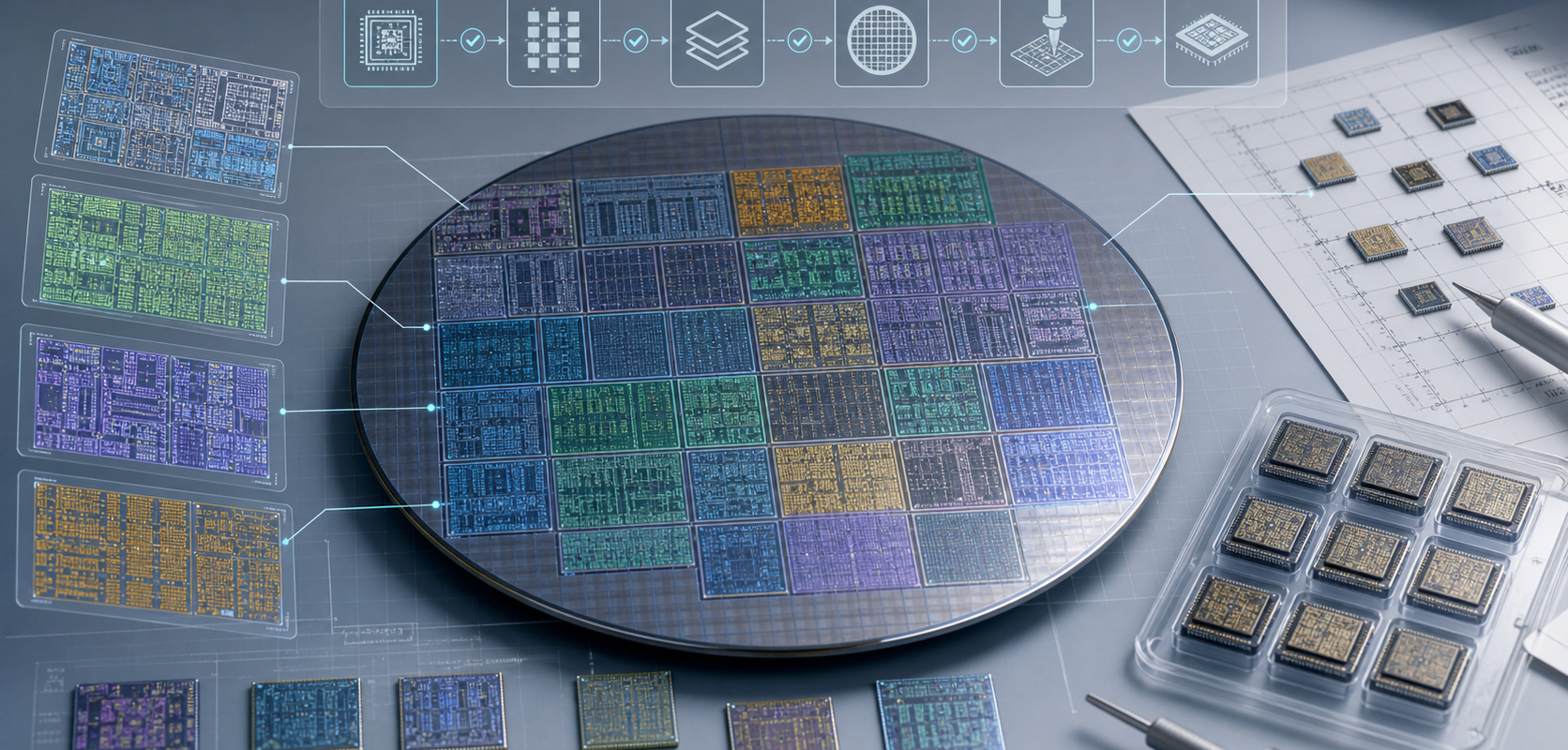
Answer-first summary: MPW means multi-project wafer. Multiple chip designs share wafer or mask resources so each team can obtain prototype silicon before committing to a dedicated full-mask route. A first MPW RFQ should start from non-confidential requirements, not GDS or design IP.
MPW stands for multi-project wafer. In an MPW run, several chip designs share manufacturing resources so early silicon access becomes more practical than paying for a dedicated full-mask route at the first step.
MPW is also called shuttle tapeout or shared-reticle prototyping. The practical idea is the same: the team uses a shared route to learn from real silicon before deciding whether a later engineering run, full mask or production path makes sense.
When MPW makes sense
MPW is useful when the design team needs real silicon but is not yet ready for a dedicated production mask set. Typical cases include analog and mixed-signal prototypes, RF and sensor interfaces, high-voltage or BCD concepts, industrial IoT chips, university research chips and early customer demonstration samples.
The common pattern is uncertainty. The team may know the target function and approximate die size, but still needs to confirm silicon behavior, package choice, probe strategy, timeline, test scope and cost.
What MPW can help prove
An MPW run can support first-silicon learning: circuit behavior, process fit, pad and IO assumptions, package/test direction, customer demo samples, measurement plans and whether the design should move toward a second revision or a more dedicated route.
It does not automatically solve product readiness. A successful MPW result still needs characterization, debug, package and test review, engineering-run planning and a commercial decision about the next stage.
What information is needed first
An early MPW RFQ does not need to start with confidential layout data. A useful first brief can include:
- target node or acceptable node range
- process family such as analog, mixed-signal, RF, BCD, high-voltage, eNVM or sensor interface
- estimated die area
- expected sample quantity
- packaging and wafer probe assumptions
- target timeline
- company country or region and end-use context
This outline is enough for a first screen. Detailed design files should move later, under the right NDA, PDK and partner-confirmed review path.
Where teams get confused
Teams often treat MPW as a simple price request. In practice, the route depends on process family, package/test scope, design maturity, PDK access, eligibility, geography, sample logistics and what the team needs to prove after first silicon.
That is why a good MPW process starts by structuring the RFQ, not by asking the buyer to upload every design file immediately.
How MST supports MPW questions
MST coordinates mature-node MPW RFQs by screening high-level requirements, clarifying the NDA and PDK path, preparing package/probe/test questions and routing qualified requests toward partner-confirmed next steps. The first conversation should stay non-confidential.
FAQ
Is MPW only for universities?
No. MPW is used by universities, fabless companies, design-service teams, research groups and industrial chip developers when prototype silicon is needed before a dedicated production route.
Do I need to upload GDS to start an MPW RFQ?
No. The first screen can start from high-level requirements only. GDS, netlist, RTL and confidential design files should not be sent at intake.
Is MPW cheaper than a full-mask route?
Often for prototypes, because resources are shared. Final cost depends on node, die area, process options, packaging, probe, test and schedule.
Next step: If you are exploring MPW, start with a high-level brief: node range, process family, die area, sample target, package/test assumptions and timeline.
Related Articles


Ready to plan your MPW and first-silicon path?
Start with a non-confidential brief covering node/process fit, schedule, first-silicon validation, packaging/test, sample handling or re-spin needs. MST routes the request for review; feasibility, availability, timing and quotation are confirmed case by case.