- →The Cpk Ceiling: Why 1.33 Feels Like a Wall
- →Understanding What Cpk Actually Measures (and What It Hides)
- →Why Traditional SPC Cannot Fix W2W Drift
- →Virtual Metrology: Seeing Every Wafer Without Measuring It
- →Run-to-Run Control: Closing the Loop
Key Takeaways
- A Cpk stuck between 1.0 and 1.67 almost always traces back to uncompensated wafer-to-wafer (W2W) drift — not random noise — meaning it is correctable with closed-loop VM/R2R control.
- Virtual Metrology (VM) predicts post-process results from equipment sensor data in real time, while Run-to-Run (R2R) feeds those predictions back to auto-adjust recipes, reducing W2W sigma by 30-60%.
- Major equipment OEMs (Applied Materials, Lam, Tokyo Electron) offer built-in APC, but these solutions are locked to their own chambers — fabs running mixed fleets need a vendor-agnostic approach.
- ‘MST’s NeuroBox E3200 is designed to deliver VM + R2R + FDC at sub-50ms edge latency (design target).’, connecting to any equipment vendor’s tool via standard SECS/GEM or EDA interfaces, without requiring the OEM’s cooperation.
The Cpk Ceiling: Why 1.33 Feels Like a Wall
You have tuned your etch recipe for weeks. Chamber matching looks reasonable. Your preventive maintenance schedule is tight. And yet, when you pull the SPC chart for critical dimension (CD) uniformity, the Cpk hovers around 1.2 to 1.4. Some lots push past 1.5. Others dip below 1.0 after a chamber clean or target change. The monthly report says “Cpk = 1.33 average,” but you know that average hides a bimodal distribution no one wants to talk about.
This is not a rare problem. It is the default state of most advanced fabs running nodes at 28nm and below. And the root cause is almost never what the SPC software flags.
Let us break down why your Cpk is stuck — and what it actually takes to push through 1.67 and hold it there.
Understanding What Cpk Actually Measures (and What It Hides)
Cpk is a capability index that captures how centered and tight your process distribution sits relative to the spec limits. A Cpk of 1.33 means your process mean is at least 4 sigma from the nearest spec limit. A Cpk of 1.67 means 5 sigma. The math is simple:
Cpk = min[(USL - mean), (mean - LSL)] / (3 * sigma)
The problem is that Cpk is calculated from the total observed variation — which lumps together within-wafer (WIW), wafer-to-wafer (W2W), lot-to-lot (L2L), and chamber-to-chamber (C2C) components. When you see a Cpk of 1.2, you are seeing the superposition of all four variance sources. But they have very different root causes and very different solutions.
The variance decomposition most fabs skip
Run a nested ANOVA on your CD or film thickness data. In a typical CVD TEOS oxide process at a mature 28nm fab, you will see something like this:
- Within-wafer (WIW): 15-25% of total variance — driven by showerhead design, temperature gradient, gas flow distribution. Hardware-limited. You cannot fix this with software.
- Wafer-to-wafer (W2W): 35-50% of total variance — driven by chamber state drift (seasoning, byproduct buildup, consumable wear), incoming wafer variation, and recipe-to-hardware interaction.
- Lot-to-lot (L2L): 10-20% — driven by incoming film stack variation from upstream steps, queue time effects, and ambient conditions.
- Chamber-to-chamber (C2C): 10-25% — driven by hardware differences between nominally identical chambers, different PM histories, and different consumable ages.
Here is the critical insight: W2W variation is typically the single largest contributor, and it is the one most amenable to real-time correction. WIW is a hardware problem — you need a better showerhead or ESC design. C2C is a matching problem that requires careful fleet management. But W2W drift is a control problem, and control problems have control solutions.
Why Traditional SPC Cannot Fix W2W Drift
Statistical Process Control was designed to detect out-of-control conditions — not to prevent them. An SPC chart with Western Electric rules will flag a shift after 7-8 consecutive points on one side of the center line. By that time, you have already processed 7-8 wafers with a shifted mean. At $500-$5,000 per wafer (depending on the node and layer), that is $3,500-$40,000 in yield risk before you even get an alarm.
More fundamentally, SPC is a detection tool. It tells you something changed. It does not tell you why, and it certainly does not adjust your recipe to compensate. The engineer gets a page, walks to the tool, reviews sensor traces, decides on an adjustment, qualifies it, and pushes the change — a cycle that takes hours to days. Meanwhile, the tool keeps running the old recipe.
The metrology bottleneck
The other structural problem is metrology sampling. Most fabs measure 1 in 5 to 1 in 25 wafers for process control metrics. For a CD-SEM measurement after etch, you might measure 9 sites on 3 wafers per lot of 25. That gives you 27 data points to characterize a lot — and zero data on the other 22 wafers. If wafer #7 drifted because the chamber had a micro-particle event between wafers #6 and #7, you will never know unless #7 happened to be a sampled wafer.
This is the metrology gap that makes Cpk improvement feel impossible: you cannot control what you cannot see, and you cannot see 80-95% of your wafers.
Virtual Metrology: Seeing Every Wafer Without Measuring It
Virtual Metrology (VM) closes the measurement gap by predicting post-process wafer parameters from equipment sensor data — the data you already collect but probably do not use for control.
A modern etch chamber generates 50-200 sensor channels at 1-10Hz: RF forward/reflected power, DC bias, chamber pressure, gas flows (multiple species), ESC temperature (multiple zones), optical emission spectra (if equipped), and endpoint signals. A single wafer process of 60 seconds produces 3,000-120,000 data points. That sensor trace is a fingerprint of exactly what happened to that wafer in the chamber.
A VM model — typically an ensemble of regularized regression, gradient-boosted trees, or shallow neural networks — learns the mapping from sensor traces to metrology outcomes. Once trained on 30-100 wafers of paired sensor + metrology data, the model can predict CD, film thickness, etch depth, or removal rate for every wafer, in real time, with no additional metrology cost.
What good VM accuracy looks like
Industry benchmarks and published results consistently show:
- CVD film thickness: VM prediction error (RMSE) of 0.3-0.8% of target, vs. measurement tool repeatability of 0.1-0.3%. Effectively, the VM prediction is within 2-3x of the measurement noise floor.
- Etch CD: VM RMSE of 0.5-1.5nm on a 50nm target, compared to CD-SEM repeatability of 0.3-0.5nm.
- CMP removal rate: VM RMSE of 50-150 A/min on a 3000 A/min process, or about 2-5% relative error.
Is this as good as measuring every wafer? No. But it is infinitely better than measuring none of them. And it is good enough to drive a R2R controller.
Run-to-Run Control: Closing the Loop
VM tells you what happened. R2R decides what to do about it.
A Run-to-Run controller takes the VM prediction (or actual metrology when available) and adjusts controllable recipe parameters for the next wafer or lot. The classic R2R architecture is an EWMA (Exponentially Weighted Moving Average) controller:
Recipe_offset(n+1) = lambda * (Target - Actual(n)) + (1 - lambda) * Recipe_offset(n)
where lambda (0 < lambda < 1) controls how aggressively the controller reacts. A lambda of 0.3-0.5 is typical — fast enough to track drift, slow enough to not chase noise.
In practice, modern R2R systems use more sophisticated approaches: multivariate EWMA (MEWMA) for correlated parameters, disturbance observers for nonlinear drift, and constraint-aware optimization that respects recipe limits and equipment capabilities. But the core idea is simple: measure (or predict), compare to target, adjust, repeat.
The Cpk math with R2R in the loop
Let us work a concrete example. Consider a PECVD silicon nitride process with a target thickness of 1000A and spec limits of 950-1050A (USL-LSL = 100A).
Without R2R:
- W2W sigma: 12A (dominated by chamber seasoning drift)
- Total sigma (including WIW and other sources): 16A
- Cpk = 50 / (3 * 16) = 1.04
With VM + R2R compensating W2W drift:
- W2W sigma reduced from 12A to 5A (R2R removes ~60% of W2W variance)
- Total sigma: sqrt(5^2 + 10^2) = 11.2A (WIW and other components unchanged)
- Cpk = 50 / (3 * 11.2) = 1.49
With VM + R2R + chamber matching (C2C compensation):
- Total sigma: 9.5A
- Cpk = 50 / (3 * 9.5) = 1.75
That is the difference between a process that fails customer audit (Cpk < 1.33) and one that passes with margin (Cpk > 1.67). And the physics did not change. The hardware did not change. What changed is that you closed the control loop.
Why Most Fabs Have Not Done This Yet
If VM/R2R is so effective, why is adoption still patchy outside of the top 5 fabs? Three reasons:
1. OEM lock-in
The equipment OEMs have advanced process control (APC) solutions: Applied Materials has Smartfab/ChamberAI, Lam has their Equipment Intelligence suite, Tokyo Electron has their own APC stack. These work — but only on that OEM’s equipment. A fab running Applied etch, Lam CVD, and TEL diffusion would need three separate APC ecosystems, three sets of integrations, three support contracts, and three different user interfaces for their engineers.
In practice, this means most fabs deploy OEM APC only on their most critical (and most painful) tools, leaving 60-80% of their equipment fleet uncontrolled.
2. Integration complexity
Connecting a VM/R2R system to equipment requires access to high-frequency sensor data (via SECS/GEM, EDA/Interface A, or proprietary interfaces), a real-time data pipeline, model training infrastructure, and a recipe management system that can accept and apply recipe offsets. Traditional approaches require months of IT/OT integration work, factory network approvals, and MES system modifications.
3. Organizational resistance
Handing recipe control to an algorithm is a cultural shift. Process engineers have spent years tuning their recipes by hand. Asking them to trust a model requires not just technical proof but also transparency: the engineer needs to see what the model is doing, why it made a specific adjustment, and have a one-click override when it gets it wrong. Black-box AI does not work on the fab floor.
The Competitive Landscape: Who Offers What
The VM/R2R market has evolved significantly in the last few years. Here is an honest assessment of the major players:
- Applied Materials (ChamberAI / Enlight): Deep integration with Applied’s own equipment. Excellent sensor access on their tools. But locked to Applied chambers — if your critical bottleneck is a competitor’s tool, this does not help.
- Tignis (acquired by Cohu): Software-focused approach with physics-informed ML models. Strong in CMP and etch applications. Good technology, but Cohu’s focus is primarily test and inspection, so semiconductor process control is not their core business.
- PDF Solutions (Exensio): Broad analytics platform with FDC and some VM capability. Strong in data infrastructure and yield analytics. Less focused on real-time, sub-second R2R control at the edge.
- Onto Innovation: Primarily a metrology company that has added analytics. Strong when you need to tie VM directly to their metrology tools. Less relevant if your metrology fleet is from other vendors.
The gap in the market is clear: there is no dominant vendor-agnostic, edge-deployed VM/R2R platform that works across all equipment brands with sub-second latency. The OEMs own their own ecosystem. The software companies are either cloud-focused or narrowly specialized.
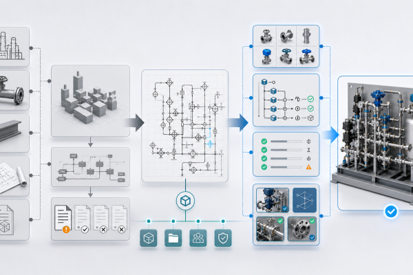
A Vendor-Agnostic Approach: What It Looks Like in Practice
MST built the NeuroBox E3200 specifically to fill this gap. The design principles reflect the real-world constraints we just discussed:
Edge deployment, not cloud
The E3200 runs at the equipment — physically deployed next to the tool or in the subfab. VM inference runs in under 50ms, which means R2R recipe adjustments are ready before the next wafer loads. There is no round-trip to a cloud server, no factory network bandwidth constraint, and no dependency on external connectivity. For a process with 60-second wafer cycle time, 50ms is invisible.
Universal equipment connectivity
The system connects to any equipment that speaks SECS/GEM (SEMI E5/E37), EDA/Interface A (SEMI E120/E125/E132/E134), or OPC-UA. That covers the vast majority of 200mm and 300mm equipment from any OEM. No need for the equipment vendor’s cooperation or proprietary API access — the data comes through standard semiconductor interfaces.
Integrated VM + R2R + FDC in one platform
Running VM, R2R, and Fault Detection on separate systems from different vendors creates integration nightmares. The E3200 runs all three on the same edge device, sharing the same data pipeline and the same equipment connection. When the FDC module detects an anomaly, it can automatically gate the R2R controller to prevent it from compensating for what is actually a fault — a common failure mode in decoupled VM/R2R/FDC architectures.
Transparent models with engineer override
Every VM prediction and R2R adjustment is logged with full explainability — which sensor features drove the prediction, what the confidence interval is, and what the model uncertainty looks like. Engineers can set guardrails (maximum recipe offset per step, maximum cumulative drift before alarm), monitor model health, and override any adjustment with a single click. The system is a tool for engineers, not a replacement for them.
Implementation: What a Realistic Timeline Looks Like
One of the biggest misconceptions about VM/R2R is that it requires a massive upfront investment and a year-long deployment. Here is what a phased rollout actually looks like:
Phase 1: Data collection and VM (Weeks 1-4)
- Connect to equipment sensor data via SECS/GEM or EDA
- Collect 30-100 wafers of paired sensor + metrology data
- Train and validate VM models offline
- Deploy VM in monitoring mode — predictions logged but no control action
- Engineers compare VM predictions to actual metrology to build trust
Phase 2: R2R in shadow mode (Weeks 4-8)
- Enable R2R controller in “advisory” mode — it calculates recipe adjustments but does not apply them
- Engineers review recommended adjustments alongside actual SPC data
- Tune controller gains (lambda, constraints) based on observed behavior
- Run parallel: actual production with manual control vs. what R2R would have done
Phase 3: Closed-loop control (Weeks 8-12)
- Enable R2R with conservative gains (low lambda, tight offset limits)
- Gradually widen controller authority as confidence builds
- Monitor Cpk improvement on controlled vs. uncontrolled chambers
- Expand to additional tools and process steps
Total time from installation to closed-loop control on the first tool: 8-12 weeks. Not 12 months. The limiting factor is usually the time needed to collect enough paired data and for the engineering team to build confidence in the system — not the technology.
When Smart DOE Matters: Getting the Recipe Right Before You Control It
VM/R2R can compensate for drift around a recipe setpoint. But if the recipe itself is poorly optimized — if the process window is too narrow or the sensitivity to controllable parameters is too low — then R2R is fighting with one hand tied behind its back.
This is where equipment commissioning and DOE (Design of Experiments) come in. Traditional full-factorial DOE for a process with 6 factors at 3 levels requires 729 runs. Even a fractional factorial or response surface design needs 50-100 wafers. At $1,000-$5,000 per wafer, that is $50,000-$500,000 in trial wafers per chamber.
MST’s NeuroBox E5200 takes a different approach: Frame as a design target / offline-lab result rather than a flat achieved fact.. The algorithm chooses each next experiment based on what it has learned from all previous ones, focusing exploration on the regions of the parameter space that matter most. Tier it: ‘In offline-lab testing, Smart DOE targets up to an ~80% reduction in trial wafers (Design Target / Measured Offline-Lab)’. — which then makes the R2R controller’s job easier.
Think of it this way: E5200 finds the best recipe. E3200 keeps it there.
The Bottom Line: Cpk Is a Control Problem
If your Cpk is stuck below 1.67, the most likely reason is uncompensated wafer-to-wafer variation from chamber state drift. This is not a hardware limitation. It is not a “we need better equipment” problem. It is a feedback control problem, and it has been solved in theory for decades. What has changed in the last few years is that the practical barriers — equipment connectivity, model accuracy, edge computing capability, deployment complexity — have finally come down enough to make VM/R2R viable for fabs of all sizes, not just the top 5.
The path from Cpk 1.2 to Cpk 1.67+ is not a mystery. It is: decompose your variance, identify the controllable components (usually W2W drift), deploy VM to see every wafer, close the loop with R2R, and iterate. The technology exists. The question is whether your fab is willing to close the loop.
About MST: Moore Solution Technology (MST) builds AI infrastructure for semiconductor equipment — from design to high-volume manufacturing. Reword to capability/intent: ‘The NeuroBox platform is designed for etch, CVD, PVD, CMP, diffusion, and lithography track applications.’ (or ‘is applicable to’) If you are evaluating VM/R2R for your fab or equipment, we are happy to walk through a technical assessment of your specific process. Reach out at sales@mst-sg.com or visit mst-sg.com.
Move from raw logs to replayable engineering evidence
Share the equipment type, legacy interface, target Host expectation and one representative incident or acceptance scenario. MST will review whether a private mapping, trace/replay or validation pilot is appropriate.
Request private evaluation →