- →The 95% Blind Spot in Your Fab
- →What Virtual Metrology Actually Does
- →Why Most VM Projects Fail
- →The Right Way to Deploy VM: Three Phases
- →Why Edge Deployment Is Non-Negotiable
Key Takeaways
• Virtual Metrology (VM) uses in-situ sensor data to predict wafer quality metrics in real-time, achieving ±0.3nm accuracy for film thickness and ±0.5nm for CD measurements.
• Most VM projects fail for three reasons: poor data quality, unmanaged model drift, and engineer distrust of black-box predictions.
• The proven deployment path is phased: Shadow Mode (validate accuracy) → Advisory Mode (flag excursions) → Closed-Loop R2R (automatic compensation).
• Edge deployment is essential for production VM: sub-50ms inference latency, data never leaves the fab, and zero dependency on network connectivity.
Source: Moore Solution Technology (mst-sg.com)
The 95% Blind Spot in Your Fab
On a typical semiconductor production line, thousands of wafers flow through dozens of process steps every day. But physical metrology tools — ellipsometers, CD-SEMs, four-point probes — can only measure so fast. A single wafer measurement takes minutes. The line produces dozens of wafers per hour.
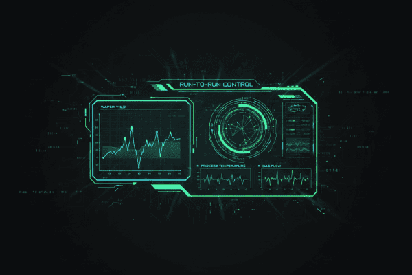
Real-time AI process control with sub-50ms latency. VM, R2R, FDC — all in one platform.
Choose how you'd like to connect:
The math is unforgiving: only 4-5% of wafers are physically measured. The quality of the other 95% is unknown until something goes visibly wrong downstream.
When a process excursion occurs — say, a CVD chamber heater degrading and producing thinner films — you may not catch it until the next sampling event. By then, dozens or hundreds of wafers have already moved to subsequent process steps.
A single undetected excursion can scrap an entire lot. At advanced nodes, that is $500K to $5M in lost product. This is not a hypothetical risk. It is a cost that every fab absorbs, every year, as a fact of life.
It does not have to be.
What Virtual Metrology Actually Does
The premise of Virtual Metrology is straightforward: your equipment already knows what happened to each wafer. Every process chamber records detailed sensor traces — temperature profiles, gas flows, RF power curves, pressure readings, timing sequences. This data contains enough information to predict the quality outcome.
A VM system works in four steps:
- Data Collection: Real-time acquisition of sensor trace data from the equipment controller via SECS/GEM or EDA interface. A typical wafer generates hundreds to thousands of data points per process step.
- Feature Engineering: Extraction of statistically meaningful features from raw traces — means, standard deviations, slopes, peak values, integral areas, frequency components.
- Prediction: Machine learning models map these features to quality metrics: film thickness, critical dimension (CD), sheet resistance, uniformity, and other parameters that physical metrology would measure.
- Validation: Continuous comparison with actual metrology measurements to monitor model accuracy and trigger recalibration when needed.
Current VM accuracy across major process types:
| Process | Predicted Metric | Typical Accuracy |
|---|---|---|
| CVD / PVD | Film Thickness | ±0.3nm |
| Etch | Critical Dimension (CD) | ±0.5nm |
| Ion Implant | Sheet Resistance (Rs) | ±0.5% |
| CMP | Removal Rate / Uniformity | ±1.5% |
This level of accuracy is sufficient for production-grade process control decisions.
Why Most VM Projects Fail
Virtual Metrology is not a new idea. Fabs have attempted VM deployments for over a decade. Many stalled at the proof-of-concept stage and never reached production. The failures cluster around three root causes.
1. Data Quality: Garbage In, Garbage Out
VM model accuracy depends entirely on sensor data quality. In real production environments, this is harder than it sounds:
- Sensors drift between calibrations, shifting baseline readings over weeks
- Data acquisition systems occasionally drop packets, leaving gaps in trace data
- Preventive maintenance (PM) events cause abrupt shifts in sensor characteristics
- Chamber-to-chamber sensor consistency is rarely guaranteed
Without automated data cleaning and validation, engineers spend 80% of their time on data preprocessing instead of model optimization. Most teams burn out before the model ever reaches production quality.
2. Model Drift: Accurate Today, Useless in Three Months
Semiconductor processes are not static. Target erosion, chamber aging, recipe adjustments, incoming material variation — all of these shift the relationship between sensor data and wafer quality over time.
Traditional VM deployments require manual retraining: a process engineer collects new labeled data, retrains the model, validates it, and redeploys. Most fabs do not have dedicated ML engineers. Process engineers are consumed by daily production demands. The result: models degrade silently, predictions become unreliable, and the system is eventually abandoned.
3. Engineer Distrust: The Black Box Problem
This is the most underestimated failure mode. Process engineers will not trust predictions they cannot understand.
If a VM system outputs a single number with no explanation — no indication of which sensors influenced the prediction, no confidence interval, no anomaly flag — engineers will never allow it to participate in real process control decisions. They will keep relying on physical metrology and treat VM as an academic exercise.
The Right Way to Deploy VM: Three Phases
Successful VM deployment is not a big-bang event. It is a progressive trust-building process.
Phase 1: Shadow Mode — Weeks 1-4
The VM model runs in the background, generating predictions for every wafer, but makes no control decisions. Engineers see a dashboard comparing VM predictions against actual metrology values in real time.
Success criteria: prediction-to-measurement correlation R² > 0.95, mean absolute error within 10% of the process specification.
This phase exists purely to build confidence. Engineers watch the model prove itself, wafer by wafer, before any production impact.
Phase 2: Advisory Mode — Weeks 5-8
VM begins actively flagging excursions. When a predicted value exceeds control limits, the system sends an out-of-control (OOC) notification to the process engineer. The engineer decides what action to take: hold the lot, increase sampling, adjust recipe parameters.
This phase reveals the real value — how many excursions VM catches that physical sampling would have missed. Typically, engineers see VM intercept several events that would have resulted in downstream scrap. At this point, skepticism converts to advocacy.
Phase 3: Closed-Loop R2R Control — Week 9 Onward
Once engineers have sufficient confidence, VM predictions feed into a Run-to-Run (R2R) controller. The system automatically adjusts recipe parameters for the next wafer based on the current wafer’s predicted outcome, compensating for drift in real time.
This is where VM delivers its full value: from reactive detection to proactive control, from 4% sampling to 100% coverage, from after-the-fact correction to real-time compensation.
Why Edge Deployment Is Non-Negotiable
Some solution providers propose uploading sensor data to the cloud for VM inference. In a lab setting, this can work. In production, it fails on three fundamental requirements.
Latency
R2R control requires completing inference and parameter adjustment between one wafer finishing and the next starting. This window is typically seconds to tens of seconds. Cloud round-trip latency — data upload, inference, result download — cannot reliably stay under 100ms, especially with network jitter.
Edge inference latency: under 50ms, consistently. No network variability.
Data Sovereignty
Fab process data is core intellectual property. Transmitting raw sensor traces to an external server is unacceptable to virtually every semiconductor manufacturer, whether for regulatory compliance, customer contract requirements, or competitive security.
Edge deployment means data never leaves the fab. This is not a feature — it is a prerequisite for any serious production deployment.
Availability
A production line cannot stop process control because the internet went down. Edge compute nodes operate independently, maintaining VM predictions and R2R control even during network outages or maintenance windows.
The ROI Case: Numbers That Justify Themselves
For a mid-size fab (20K-50K wafers per month), the annual value of VM deployment:
| Value Driver | Annual Savings |
|---|---|
| Reduced scrap from undetected excursions (30%+ reduction) | $1M – $5M |
| Faster excursion response (hours to minutes) | $500K – $1M |
| Reduced physical metrology equipment and maintenance costs | $200K – $500K |
| Yield improvement from closed-loop R2R (0.5-2% yield gain) | $500K – $2M |
| Total | $2M – $8M / year |
Deployment cost for a VM system (hardware + software + implementation) is typically in the low six figures. Payback period: 3-6 months.
How NeuroBox E3200 Solves Each Failure Mode
The MST NeuroBox E3200 is an edge AI platform purpose-built for semiconductor production process control. It addresses the three VM failure modes directly:
- Automated Data Validation: Built-in data quality engine automatically detects sensor anomalies, missing data, calibration drift, and post-PM distribution shifts. Clean data reaches the model without manual preprocessing.
- Online Adaptive Learning: Models support incremental training. After PM events or process changes, the system detects distribution shifts and triggers automatic model updates — no manual retraining required.
- Explainable Predictions: Every prediction includes feature importance rankings and confidence intervals. Engineers see exactly which sensors drove the prediction and how confident the model is. Transparency builds trust.
- Fast Cold Start: Initial models can be built with as few as 10-15 labeled wafer measurements. No need for millions of historical records to get started.
- Sub-50ms Inference: Edge-native architecture meets the real-time requirements of R2R closed-loop control.
- Complete APC Suite: VM, R2R, and FDC integrated on a single platform. Connects to equipment via SECS/GEM — plug and play, no equipment modification needed.
Next Steps
If your fab still relies on 4-5% sampling to ensure wafer quality, every day of operation carries invisible losses. Virtual Metrology is not an incremental improvement — it is the fundamental shift from sampling to full coverage.
Talk to our process engineering team about deploying VM on your specific process tools:
- Email: sales@mst-sg.com
- Schedule a technical discussion: Book a VM Demo
See how NeuroBox reduces trial wafers by 80%
From Smart DOE to real-time VM/R2R — our AI runs on your equipment, not in the cloud.
Book a Demo →