
How to Tapeout a Chip: From Final GDS to FAB Out and First Silicon
A practical tapeout guide from process and PDK readiness through final GDS, data acceptance, wafer fabrication, FAB Out, packaging, test and first silicon.

Short answer: Final GDS submission is not the same as Tape Out or Wafer Start. After provider or foundry data acceptance, an MPW run may move through mask-data preparation and mask release before wafer fabrication. FAB Out means front-end wafer processing is complete under the provider’s definition; wafer sort, dicing, packaging, final test and sample shipment may still follow.
Tapeout is an engineering release path, not a single upload. A useful plan connects process choice, PDK access, signoff, the final layout handoff, the shared MPW run, wafer manufacturing and the work required to turn fabricated die into testable first silicon. The exact names, order and visibility of milestones vary by provider and process.
Step 1: Choose the process family before the node
A node number alone is not enough. A mature-node logic shuttle, BCD option, RF process and high-voltage mixed-signal route are not interchangeable. Start with the circuit requirement: supply voltage, analog precision, RF range, device options, memory need, IO, sensor interface, reliability conditions and package constraints.
Step 2: Confirm the PDK and NDA path
Serious tapeout work needs the correct process design kit, rule decks and signoff expectations. Some educational programs publish open flows; many commercial routes require eligibility review and an NDA before PDK access. A first screening brief can start without GDS, but implementation cannot be released against rules that have not been identified and controlled.
Step 3: Build the design with signoff in mind
Architecture, simulation, synthesis, place-and-route, custom layout, IO planning and pad-ring choices all affect final release. Verification is not a final-week activity. DRC, LVS, ERC, antenna, density, latch-up, ESD, timing, power integrity and reliability assumptions need owners, tool versions and a documented waiver policy.
Step 4: Prepare the final GDS/OASIS handoff
The final layout handoff normally includes a manifest with the process and option, top cell, units, layer-map reference, signoff status, excluded cells, known waivers, checksum, release date and owner. The Local GDSII Inspector can inspect high-level file structure in the browser without uploading layout data, but it does not replace provider or foundry checks.
Step 5: Lock package and test assumptions early
First silicon is useful only if the team can probe, power, package and test it. Package outline, pad or bump map, pinout, thermal assumptions, wafer probe, dicing, sample quantity, test hardware and logistics should be scoped before the design is frozen. See MPW Packaging, Wafer Probe and Test: Specify Early for the downstream checklist.
After final GDS: customer-visible and internal milestones
Customer-visible milestones and foundry-internal work are related, but they are not the same status chain. Official MPW schedules commonly separate dry-run or preliminary GDS, final GDS, run tapeout and estimated shipment. Data review can loop; mask preparation activities can be coupled or parallel; wafer manufacturing contains repeated inline measurement and hold decisions.
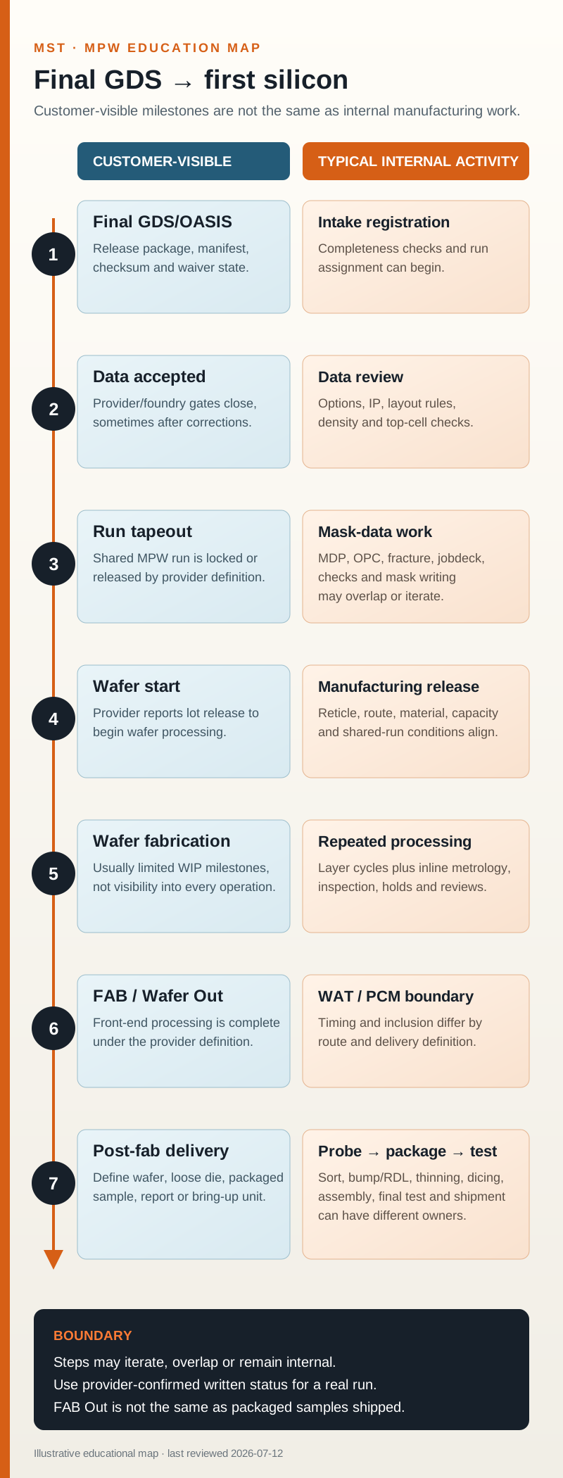
| Customer-visible milestone | Typical internal activity | Change boundary and customer evidence |
|---|---|---|
| 1. Final GDS/OASIS Release package, manifest, checksum and signoff or waiver state are frozen. |
Provider intake registration, completeness checks and run assignment may begin. | An upload is not yet Data accepted, Run tapeout or Wafer start. Keep the exact submitted revision. |
| 2. Data accepted The provider or foundry closes the applicable data-review gates, sometimes after a correction loop. |
Process-option, IP, density, layout-rule, top-cell and manufacturing-data checks vary by route. | Customer evidence should be a written provider status. MST pre-screening is not foundry acceptance. |
| 3. Run tapeout / mask release The shared MPW run is locked or released under the provider’s definition. |
Typical mask-data work can include MDP, OPC, fracture, jobdeck preparation, mask-rule checks and mask writing; activities may overlap or iterate. | Late changes require provider review and can move a design to another run. Use the provider’s named milestone. |
| 4. Wafer start The provider reports that the lot has been released to begin wafer processing under its milestone definition. |
Reticle readiness, route, material, capacity and shared-run conditions influence when processing starts. | Treat dates as provider-confirmed estimates, not as a status inferred from a submitted file. |
| 5. Wafer fabrication Customers may receive limited WIP milestones rather than visibility into every operation. |
Deposition, lithography, etch, implantation, clean and CMP repeat across layers. Inline metrology and inspection feed hold, review, rework or scrap decisions. | Progress is not proof of function or yield. Keep package, probe and bring-up work moving in parallel. |
| 6. FAB / Wafer Out Front-end wafer processing is complete under the provider’s definition. |
WAT or PCM timing and inclusion differ by route and delivery definition. | FAB Out does not by itself mean packaged parts, final-test results, shipped samples or working silicon. |
| 7. Post-fab The delivery path may include wafer sort, bump or RDL, thinning, dicing, assembly, final test, shipment and first-silicon bring-up. |
Foundry, OSAT, test house, logistics provider and customer teams can own different steps. | Define whether the deliverable is a wafer, loose die, packaged sample, test report or bring-up-ready unit. |
Boundary: this diagram is illustrative. Steps can iterate, overlap or remain internal. Availability, slot, process fit, PDK access, quotation and dates remain provider-confirmed case by case. It is not a foundry SLA.
A synthetic small-chip example: GDS to a testable sample
This illustrative synthetic example uses a small mixed-signal sensor interface with a pad ring. It contains no customer design, no proprietary PDK layer and no foundry-internal artwork. The same design intent is represented differently as GDS/OASIS hierarchy, a reticle placement, repeated dies on a wafer, a separated die and finally a package or test fixture.
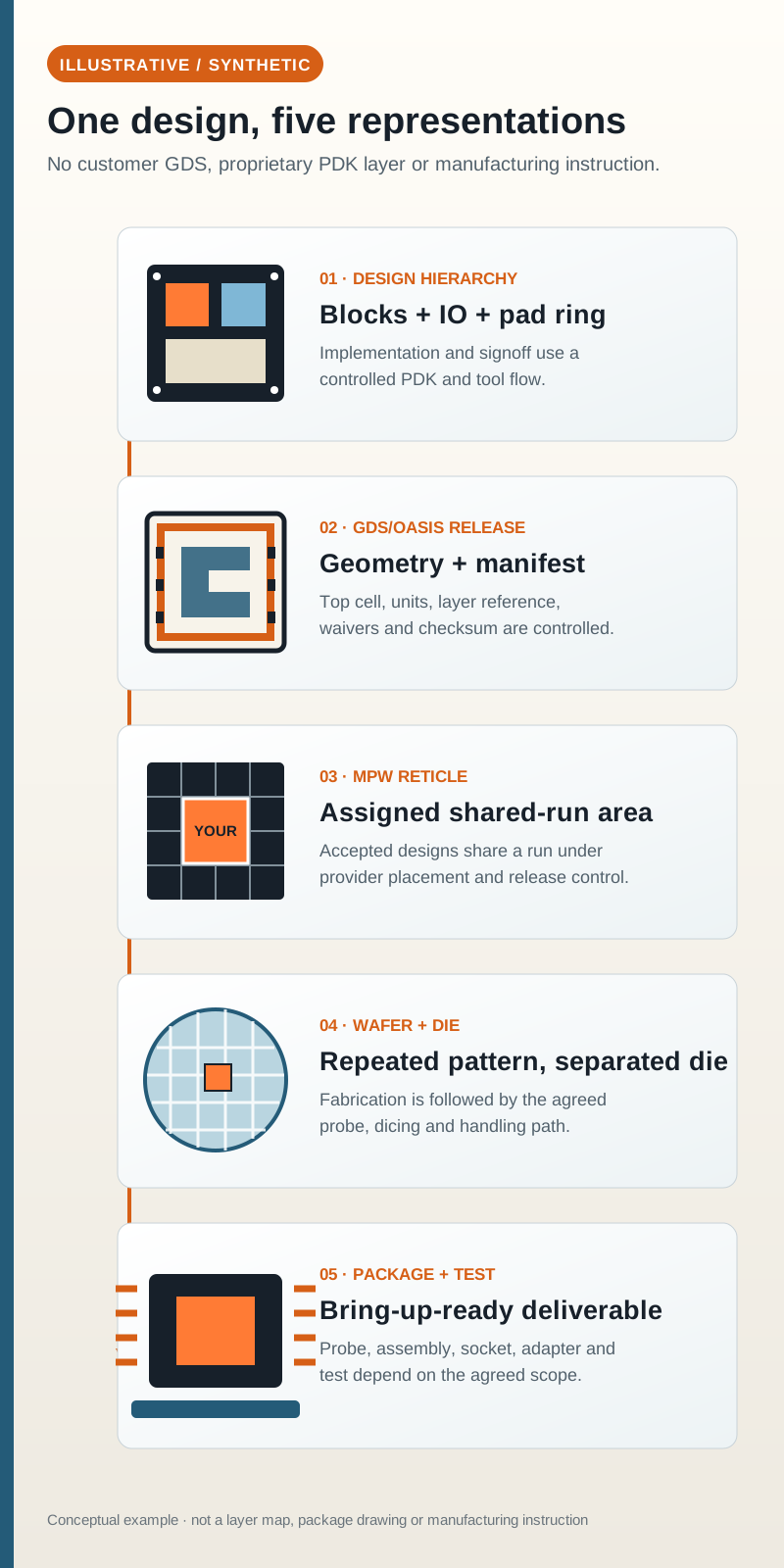
- Design hierarchy: schematics or RTL become implemented blocks, IO and a pad ring; signoff is performed against the controlled PDK and flow.
- GDS/OASIS release: the hierarchy is represented as manufacturing geometry plus a manifest and checksum. This is still data, not a wafer.
- MPW reticle placement: the accepted design occupies an assigned shared-run area alongside other designs under provider control.
- Wafer and die: the reticle pattern is repeated during wafer manufacturing; post-fab work can separate, handle and identify individual die.
- Package and test: the die may go to probe, assembly, a socket or an adapter and then first-silicon bring-up. The required path depends on the agreed deliverable.
Where do DFT, DFM, DfR and DfA fit?
| Discipline | When it starts | What continues later |
|---|---|---|
| DFT — Design for Test | Starts in architecture and RTL. Scan, BIST, JTAG, test points and test access are implemented and verified before tapeout. | ATPG, ATE program work, silicon diagnostics and coverage closure can continue during first-silicon and production preparation. |
| DFM — Design for Manufacturability | Customer-side layout rules, density, fill, hotspot review and signoff belong before release. | Foundry- or mask-side proprietary OPC, fill, slotting and MDP can occur after customer handoff. These do not repair a logically or electrically incorrect design. |
| DfR — Design for Reliability | Starts with voltage, temperature, lifetime, aging, EM/IR, ESD, latch-up and thermal assumptions. | Characterization, qualification and failure learning continue after silicon arrives. |
| DfA — Design for Assembly | If DfA means Design for Assembly, die outline, pad or bump map, package, IO and thermal-mechanical constraints should be planned before silicon release. | Assembly-process development and package qualification continue after FAB Out. Always expand the acronym so it is not confused with failure or defect analysis. |
First-silicon readiness checklist
- Process family, node range and required device options are defined.
- PDK, NDA, eligibility and signoff-tool paths are known.
- Owners exist for DRC, LVS, ERC, timing, power, reliability and waivers.
- Top cell, units, layer-map reference, checksum and release manifest are controlled.
- Package outline, pad or bump map, pinout and thermal assumptions are documented.
- Wafer probe, final test, sample quantity and the delivery form are scoped.
- The team distinguishes Final GDS, Data accepted, Run tapeout, Wafer start, FAB Out and Samples shipped.
- The first external brief contains high-level, non-confidential information only.
Run a quick Tape Out readiness check and generate a non-confidential MPW brief. Do not paste GDS/OASIS, RTL, netlists, schematics, PDK files, source code or other confidential design IP into the public tool.
Practice each step with the MPW tutorials
Use these lessons alongside the complete checklist. Each produces a small planning or handoff record you can review before the next stage.
- MPW fundamentals: write a one-page chip project brief.
- PDK preparation: identify process options, versions and open decisions.
- GDS handoff: tie reports and checksums to the exact release.
- Packaging and test: plan the samples and measurements you need.
Learning path reviewed: 16 September 2026. These exercises support preparation; they do not replace provider acceptance or engineering signoff.
Frequently asked questions
What happens after final GDS?
After final submission, the provider or foundry reviews and accepts the applicable data before the shared run is locked or released. Mask-data work, mask readiness and Wafer Start can follow under route-specific definitions. FAB Out ends front-end wafer processing, while sort, dicing, packaging, final test and shipment may still remain.
What is the difference between Final GDS and Tape Out?
Final GDS is the customer’s released layout-data package and its controlled manifest. Tape Out can mean different things across organizations: customer data release, provider run lock or mask release. An MPW project should name the specific milestone instead of assuming every party uses Tape Out for the same event.
What is the difference between Tape Out and Wafer Start?
Tape Out is a data or run-release milestone. Wafer Start is a manufacturing milestone reported under the provider’s convention. Between them, data acceptance, shared-run closure, mask-data preparation, mask readiness, planning and other gates may still occur.
When does a design change become difficult?
The boundary depends on the provider and run. A change before final submission is usually a new controlled revision; after data acceptance or run lock it requires explicit review; after mask release it can affect the assigned run and associated commercial work. Ask for the last changeable milestone in writing.
Does FAB Out include packaging and final test?
Usually, FAB Out or Wafer Out describes completion of front-end wafer processing under a provider-specific definition. Wafer sort, bump or RDL, thinning, dicing, assembly, final test and shipment can remain. The purchase order or statement of work should define the actual delivery point.
Where do DFT, DFM, DfR and DfA begin?
They begin before tapeout and overlap. DFT starts in architecture and RTL; DFM shapes implementation and signoff; DfR starts with electrical and lifetime assumptions; Design for Assembly starts with die, IO and package constraints. Post-silicon pattern work, characterization, qualification and assembly learning continue later.
Does DRC/LVS clean mean the chip will work?
No. DRC checks selected physical rules and LVS checks layout-to-netlist consistency. Clean results are necessary gates for many routes, but they do not prove the specification, models, timing, analog behavior, power integrity, reliability, test coverage, manufacturability or yield.
Primary sources and review boundary
- EUROPRACTICE 2026 MPW schedule — separates dry-run GDS, final GDS, tapeout and estimated shipment milestones.
- TSMC CyberShuttle — describes the shared MPW service model.
- Synopsys Mask Data Preparation — describes fracture, verification, mask-rule checks and jobdeck work.
- GlobalFoundries GlobalShuttle MPW program — describes a current shared-wafer service, customer variability and provider-controlled tapeout timing.
- Synopsys TestMAX DFT — places DFT across RTL, synthesis and implementation.
- ASE Test Services — covers wafer probe, sort and final-test work after wafer processing.
- UMC Turnkey Solutions — distinguishes wafer process, bumping, sorting and downstream services.
Last technically reviewed: July 12, 2026. Provider definitions, process options and schedules change. Use current provider documents and written project confirmation for an actual run.
Practice the handoff before using real design data
Work through the MPW Handoff Handbook with the downloadable exercise. Start with GDS basic inspection, identify a report bound to an old layout, create a file inventory and fill out a first-silicon test-plan template. Every exercise has an expected result.
Use Report Revision Check for declared report/layout identity, Handoff Manifest for file inventory and the existing Readiness Checker to structure missing preparation. These are preparation aids. Process fit, approved verification, submission acceptance and commercial terms still need confirmation through the relevant engineering and service owners.
Related Articles


Ready to plan your MPW and first-silicon path?
Start with a non-confidential brief covering node/process fit, schedule, first-silicon validation, packaging/test, sample handling or re-spin needs. MST routes the request for review; feasibility, availability, timing and quotation are confirmed case by case.