
BCD vs eFlash vs Logic CMOS vs SiGe BiCMOS: Which Process Fits Your Chip?
An engineering comparison of BCD, embedded flash, logic CMOS and SiGe BiCMOS using device, PDK, package, test and five buyer scenarios.
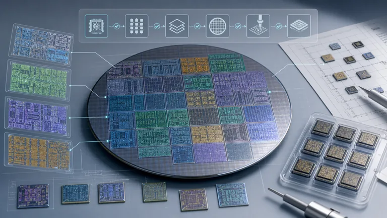
Short answer: Choose a BCD-capable platform when power/high-voltage devices and control logic must coexist; require an eFlash-capable option when on-chip reprogrammable nonvolatile memory and its programming/reliability flow are essential; emphasize logic CMOS when digital density, libraries and power-performance-area are the main drivers; and consider SiGe BiCMOS when high-performance HBT devices plus CMOS integration solve an RF, microwave or very-high-speed analog problem. These labels are screening lenses, not four mutually exclusive process families: embedded flash or other eNVM can be integrated into BCD or logic platforms. Final selection requires the actual PDK, device/model and memory-option coverage, IP, metal stack, reliability conditions, package interface and provider review.
The same application name can lead to different processes. A motor-control device may place only low-voltage control on chip and keep power external, or it may integrate 24V drivers. An RF sensor may be satisfied by CMOS RF devices at one frequency and linearity target, while another needs SiGe HBT performance and specialized passives. Process choice is a requirement-to-device-model decision.
Four capability lenses that may overlap in one platform
| Capability or platform emphasis | Primary reason to consider it | Evidence that matters | Common selection error |
|---|---|---|---|
| BCD / high-voltage mixed signal | Integrate bipolar/analog, CMOS control and DMOS or other higher-voltage devices; support power-management or actuation functions. | Required voltage and SOA, isolation, device types, on-resistance, precision models, passives, ESD, temperature and reliability. | Assuming every “180 nm” or “55 nm BCD” option supports the same voltage/device set. |
| Embedded flash / eNVM platform | Store firmware, trim, configuration or security state on chip with defined program/erase/read behavior. | Memory macro/bit-cell availability, voltage generation, endurance, retention, temperature, test/program flow, IP and licence. | Selecting eFlash because the application is called an MCU without validating capacity, endurance and programming architecture. |
| Logic CMOS | Implement digital logic with appropriate density, performance, power, libraries and IO; often with analog options where available. | Standard-cell/memory/IP portfolio, PPA targets, voltage, IO, variation, timing/signoff, metal stack and package/power delivery. | Choosing the smallest node without accounting for die IO limitation, NRE, analogue needs, IP, power or design readiness. |
| SiGe BiCMOS | Combine high-speed/low-noise SiGe HBT devices with CMOS for RF, mmWave, data-converter or high-speed interface integration. | HBT models, noise/linearity, breakdown, passives, substrate/BEOL, EM flow, package/interconnect and temperature. | Treating published fT/fmax as the achievable system frequency or product performance. |
BCD: begin with voltage domains and energy, not “power chip”
BCD platforms combine device classes so control, analog and higher-voltage functions can share a die. The first screen should list every external and internal voltage, transient, current path, switching frequency, isolation requirement, expected fault energy, temperature and lifetime condition. Then map those requirements to specific PDK devices and safe-operating-area models.
A process marketing page can show that a family spans certain application or voltage regions, but it cannot prove that the exact desired LDMOS, isolated device, precision bipolar, resistor, capacitor, OTP/eNVM, ESD structure or thick-metal option exists in the run you can access. Package thermal resistance, current-carrying interconnect and external passives may remain system constraints.
eFlash: memory technology creates a product flow
Embedded flash is not merely a storage block dropped into any CMOS process. It can introduce dedicated devices, masks, high-voltage generation, program/erase algorithms, test modes, redundancy, trim, data retention, endurance and security considerations. Ask whether the route supplies qualified memory macros or only technology devices, who owns the controller and programming algorithm, and how wafer/package test handles programming.
For an MCU-like design, quantify code and data capacity, update frequency, retention period, operating/junction temperature, write/erase cycles, read speed, security state and field-update model. A 90nm or 55nm eFlash option may be a preliminary fit, but “MCU at 55nm” is not a technical specification.
Logic CMOS: optimize the whole die and ecosystem
Digital designs are often compared by nominal node, but first-silicon success depends on the accessible ecosystem: synthesizable libraries, SRAM/compiler availability, interface IP, clocking, IO voltage, signoff tools, package power delivery and the team’s verification maturity. A smaller core can still be pad-limited; a more advanced node can increase IP, mask, EDA and implementation complexity without improving the product business case.
For generic logic, estimate gate count, memory, clocks, performance, dynamic/leakage power, die area including IO, external interfaces and test. Compare at least one mature-node implementation when schedule, mixed-signal integration or first-tapeout risk matters.
SiGe BiCMOS: RF performance is a chain, not one transistor metric
SiGe BiCMOS combines heterojunction bipolar transistors with CMOS and process-specific passives/interconnect. It can be attractive for low-noise amplifiers, power amplifiers within device limits, high-speed data converters, oscillators, transceivers and mmWave functions. Selection must use device noise, gain, linearity, breakdown, bias, temperature and model validity at the intended operating point.
Published fT and fmax characterize device technology under defined conditions; they are not the operating frequency of a complete circuit. Inductor/Q models, transmission lines, electromagnetic extraction, substrate coupling, package transition, PCB, antenna and calibration can set system performance. A run offering SiGe does not automatically include the package and measurement path needed to prove the design.
Five buyer scenarios: how preliminary screening works
Scenario A: a 24V industrial actuator or motor-control ASIC
Preliminary fit: investigate a BCD/high-voltage mixed-signal option if 24V-tolerant or higher-voltage switching/driver devices must be integrated with control and sensing. Do not infer: a nominal voltage label alone does not confirm transient SOA, isolation, on-resistance, ESD, current density or thermal feasibility. Next evidence: voltage/fault matrix, load and switching conditions, isolation topology, PDK device table, reliability rules and package thermal/current path.
Scenario B: a 90nm or 55nm eFlash MCU/control SoC
Preliminary fit: investigate the specific embedded-flash/eNVM option when field firmware, trim or configuration must be on chip. Do not infer: node plus “eFlash” does not establish memory size, macro availability, endurance, retention, programming voltage, security or test flow. Next evidence: memory use model, temperature/lifetime, access to memory IP and controller, PDK release and package/wafer programming plan.
Scenario C: a high-frequency front end considering 55nm SiGe or another SiGe platform
Preliminary fit: SiGe BiCMOS may suit noise, gain, linearity or frequency targets that benefit from HBT devices integrated with CMOS. Do not infer: the node label or device fT/fmax proves circuit bandwidth, output power or sensitivity. Next evidence: operating frequency and bandwidth, noise/linearity/power targets, HBT/passive models, EM and package/board transition plan, test-instrument capability.
Scenario D: generic logic with moderate memory and standard IO
Preliminary fit: compare logic CMOS platforms using implementable PPA, standard cells, SRAM, IO, clock/test IP, signoff flow and MPW access. Do not infer: the most advanced available node gives the lowest total project cost or fastest first silicon. Next evidence: synthesis/memory/IO estimate, package pins, power budget, IP licences, team flow maturity and total route cost.
Scenario E: MEMS, silicon photonics or another out-of-catalog device
Preliminary fit: stop the BCD/eFlash/logic/SiGe comparison and identify a technology-specific provider or integration route. Do not infer: a CMOS MPW accepts MEMS structures, special materials, post-processing or photonic layers. Next evidence: device cross-section, material/process requirements, design rules, packaging/interface and whether a published specialized MPW exists.
A process-selection decision record
| Decision input | Evidence you need | Unknown owner | Next gate |
|---|---|---|---|
| Electrical operating envelope | Voltage/current/frequency/precision/noise/temperature/lifetime requirements and transients. | System/chip architect | Candidate device families. |
| On-chip functions | Logic, analog, power, RF, memory, IO, passives, sensors and test access. | Architecture owner | Process-option shortlist. |
| PDK and model evidence | Actual devices, corners, SOA, passives, memory/IP, rule decks and supported EDA versions. | Design lead/provider | Preliminary fit approved for implementation study. |
| Die/package interaction | Area including IO, pad/bump map, power/thermal/current paths and RF transition. | Physical/package owner | Package feasibility. |
| Reliability and test | Operating mission, characterization, DFT, programming and qualification intent. | Test/quality owner | Lifecycle plan. |
| Accessible manufacturing route | Eligibility, PDK access, current run, minimum area, samples and downstream scope. | Provider/commercial owner | Provider-confirmed RFQ. |
Why the node should come later
Once a process family and device set pass the hard gates, node and implementation tradeoffs become meaningful. Compare die area, performance, power, analog headroom, voltage options, IP, design schedule, mask/MPW economics, sample delivery, production path and lifecycle. The “best” node is the one that closes the product requirements with credible models, tools, people and supply—not the smallest number.
What a safe public screening brief contains
Share high-level ranges and unknowns: application class, voltage domains, temperature, frequency, analog/RF targets, memory need, logic/memory estimate, interface types, area estimate, design stage, target quantity, delivery form and timing intent. Do not place GDS/OASIS, RTL, netlists, schematics, layouts, screenshots, PDK/rule files, detailed proprietary architecture or credentials in a public intake.
Use the MPW Node Selection Advisor to organize non-confidential requirements and the MST MPW access guide for route context. Then compare How to Choose an MPW Shuttle Run, the end-to-end steps in Small-Batch Chip Manufacturing, and access constraints in How to Tape Out Your First ASIC Without a Foundry Account. For route economics, see Where Can I Manufacture a Small Batch of Custom Chips? and MPW vs Full Mask.
Request a non-confidential chip-process fit review. MST can structure a preliminary fit and reviewed RFQ path; the actual PDK and responsible provider determine device availability, technical acceptance, access, capacity, quotation and milestones.
Frequently asked questions
Is BCD better than standard CMOS for a power-management chip?
BCD is a strong candidate when higher-voltage/power devices, analog and control logic must coexist. If the chip only controls external power devices, a logic or mixed-signal CMOS option may be sufficient. Compare the actual device set, SOA, isolation, passives and system partition.
Does an MCU always need embedded flash?
No. Firmware can reside in external memory, mask ROM, OTP, another eNVM or a companion device depending on update, cost, security and system needs. If eFlash is required, its memory and programming/reliability flow must be designed as part of the product.
Is SiGe BiCMOS only for millimeter-wave chips?
No. It can serve RF, microwave, high-speed analog and data-conversion functions where its HBT and passive options are valuable. The benefit must be shown at circuit/system level against CMOS, RF SOI or other alternatives.
Can I choose a process from the MPW calendar alone?
No. A calendar shows announced access dates and technology labels. It does not prove your device/model/IP requirements, PDK eligibility, design readiness, capacity or package/test route. Use it only after a technical shortlist.
Does a process that supports automotive applications make my chip qualified?
No. Process features and quality-system support are inputs. Product and package qualification require an application-specific plan, controlled manufacturing baseline, reliability evidence and approval; a prototype MPW part is not automatically qualified.
Primary sources and review boundary
- X-FAB BCD technology — official description of BCD integration, application space and technology range.
- X-FAB XT018 — a concrete process example showing why devices, voltages, memories, passives and options matter beyond the node.
- IHP MPW and prototyping service — official SiGe/CMOS technology and MPW access context.
- GlobalFoundries process design kits — official PDK, models, libraries, IP and design-flow context.
- EUROPRACTICE 2026 schedules and prices — current evidence that BCD, eNVM, logic and SiGe capabilities appear in different platform/run combinations with different commercial conditions.
- Automotive Electronics Council documents — qualification-document references that distinguish product evidence from a process marketing claim.
Last technically reviewed: July 30, 2026. This comparison supports preliminary screening only. Device availability, memory/IP, model validity, SOA, passives, BEOL, reliability, PDK access, packaging, test and manufacturing acceptance require the exact controlled process documentation and provider confirmation.
Related Articles

Ready to plan your MPW and first-silicon path?
Start with a non-confidential brief covering node/process fit, schedule, first-silicon validation, packaging/test, sample handling or re-spin needs. MST routes the request for review; feasibility, availability, timing and quotation are confirmed case by case.