
Small-Batch Chip Manufacturing: Process, PDK, Packaging and Test
An end-to-end small-batch ASIC guide covering process choice, controlled PDK, design release, wafer fabrication, probe, dicing, packaging, test and qualification.

Short answer: Small-batch chip manufacturing is an end-to-end engineering chain: define the product and process requirements; obtain controlled PDK, model, library and IP access; implement and sign off the design; register and release final layout data; fabricate the wafer; then plan wafer probe, dicing, packaging, final test, characterization and any required qualification. Fabricated die are not automatically packaged, tested or production-qualified parts. Name the owner, input, output and acceptance evidence for every stage before choosing an MPW or dedicated route.
Many first-chip plans are detailed until final GDS and vague afterward. That is dangerous. A chip that reaches FAB Out can still be unusable if the pad map does not match the package, no probe card or load board exists, test access is insufficient, samples cannot be identified after dicing, or bring-up has no controlled power and measurement plan.
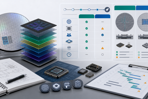
The complete chain at a glance
| Stage | Controlled input | Output or evidence | What it does not prove |
|---|---|---|---|
| 1. Product requirements | Function, interfaces, voltage, temperature, frequency, performance, reliability and sample use. | Approved engineering specification and acceptance intent. | That a suitable process or run exists. |
| 2. Process/PDK access | Entity eligibility, NDA/DKLA, process option and EDA environment. | Controlled PDK, models, rules, libraries/IP and version record. | That the design is correct or accepted for fabrication. |
| 3. Design and verification | Architecture, RTL/schematics, models, constraints and verification plan. | Functional, timing, analog, power and reliability evidence. | Physical manufacturability or final-data acceptance. |
| 4. Physical implementation/signoff | Netlist/layout, pad ring, package constraints, rule decks and waivers. | DRC/LVS/ERC and applicable signoff record plus release manifest. | That silicon will meet every specification or yield target. |
| 5. Run registration and final data | Area, quote/PO, run identity, final GDS/OASIS and checksum. | Provider data-acceptance status and run milestone evidence. | Wafer start, FAB Out or shipment unless explicitly reported. |
| 6. Wafer fabrication | Accepted manufacturing data and provider/foundry release. | Processed wafer and route-specific WAT/PCM evidence if included. | Known-good die or packaged samples. |
| 7. Probe and dicing | Wafer map, probe plan, test limits, saw streets and handling instructions. | Probe data, die map and separated die under the agreed scope. | Final packaged performance. |
| 8. Package assembly | Die drawing, pad/bump map, package design, materials and assembly flow. | Assembled engineering samples and assembly traceability. | Electrical compliance or product qualification. |
| 9. Final test/characterization | Test program, hardware, limits, conditions and correlation plan. | Tested units, data, characterization and failure evidence. | Long-term reliability or production qualification by itself. |
| 10. Qualification/production | Application-specific standards, reliability plan, process/package baseline and change control. | Qualification report and approved production controls where required. | Universal fitness for every end use. |
1. Requirements must include the post-silicon experiment
Write not only what the chip should do, but how the first samples will prove it. Identify supplies, clocks, interfaces, external components, calibration, debug access, expected current, safe power-up order, test modes and the measurements that separate a design error from a board, package or test-fixture problem.
For a small batch, every sample matters. Decide whether destructive analysis, process monitors, package cross-sections or reliability stress samples are needed so the requested quantities reflect the learning plan.
2. Select the process and lock the PDK configuration
Map requirements to the actual device catalogue and models: voltage domains, analog precision, RF performance, embedded nonvolatile memory, IO, ESD, passives, metal stack, temperature and lifetime conditions. Record the PDK release, supported EDA versions, libraries, IP, model corners and signoff decks. The process family may be a preliminary fit based on public evidence; the implementation baseline requires controlled PDK and provider review.
3. Co-design die, package and board
Package choices affect pad pitch, die size, signal integrity, power integrity, thermal path, mechanical constraints, assembly yield and test access. A cheap package that forces a larger die or cannot support the analog/RF interface may not be cheap. Lock the pad or bump map, pinout, die orientation, keep-outs and package outline before final top-level signoff.
For wire-bond designs, consider pad metallurgy, pitch, bond-finger assignment and loop constraints. For flip chip, define bump/RDL, substrate routing, underfill and assembly requirements. These are provider/OSAT-specific engineering tasks, not values inferred from the MPW node.
4. Design testability before tapeout
DFT is broader than scan. Decide how digital logic, memories, analog blocks, high-voltage sections, RF paths and trims will be observed and controlled. Plan JTAG or boundary scan if relevant, BIST, test modes, muxing, accessible monitors, calibration storage and failure diagnostics.
Separate wafer probe from final test. Probe may screen die before assembly or collect characterization, while final test validates packaged units under a different electrical and thermal environment. The test program, ATE or bench hardware, load board/probe card, sockets, limits and data format all need owners.
5. Treat final GDS as a release package
The final release should identify the exact process option, top cell, units, layer map, area, seal ring, pad/bump map revision, PDK/rule versions, signoff status, known waivers, checksum, release date and approver. Keep one immutable copy of what was accepted. Data accepted, run tapeout, wafer start and FAB Out should remain separate status fields.
6. Define what “samples delivered” means
A project plan must state whether quantities refer to gross die, expected delivered die, packaged units or units passing a specified test. It must also state whether wafer probe, dicing, bumping, packaging, final test, shipping and data reports are included. Early estimates cannot guarantee yield or final passing quantity.
7. Characterization is not qualification
Characterization explores device and product behavior across voltage, temperature, process variation and operating conditions. Qualification applies a controlled plan and acceptance criteria appropriate to the product, package, manufacturing baseline and market. A process may support automotive-oriented features or standards without making an individual product automatically AEC-qualified.
Prototype, engineering sample, characterized part, qualified product and released production part should be separate lifecycle states. Record who can approve each transition.
The end-to-end decision record
| Decision input | Evidence you need | Unknown owner | Next gate |
|---|---|---|---|
| Product use and operating envelope | Approved specification, sample learning goals and preliminary qualification intent. | Product owner | Process-family shortlist. |
| Technology configuration | Exact PDK, models, libraries, IP, EDA and signoff deck versions. | Design lead/provider | Implementation baseline. |
| Physical delivery | Wafer/die/package form, drawings, sample convention, logistics and handling. | Package owner | OSAT feasibility and quote. |
| Testability and test execution | DFT plan, probe/final-test split, hardware, program, limits and data format. | Test owner | Test readiness review. |
| Manufacturing release | Run code, commercial gates, final-data manifest and provider acceptance. | Tapeout coordinator | Provider-defined run release. |
| First-silicon acceptance | Bring-up procedure, expected signatures, characterization matrix and issue triage. | Silicon validation lead | Re-spin or next lifecycle decision. |
| Qualification/volume transition | Applicable standard, reliability matrix, baseline ownership and change-control path. | Quality/operations owner | Production release plan. |
A 12-item manufacturing readiness checklist
- The process family is justified by devices/models, not only a node.
- The exact PDK and supported tool versions are controlled.
- IP and library licences cover the project and target route.
- Signoff checks and waiver authorities are named.
- Die outline, seal ring and pad/bump map are revision-controlled.
- The package route is feasible and has a named owner.
- Probe and final-test purposes are separated.
- Test modes, hardware and program ownership are planned.
- Registration, final GDS and provider acceptance are distinct milestones.
- The sample quantity and delivery form are unambiguous.
- Bring-up and characterization have acceptance evidence.
- Qualification and production are not implied by a prototype delivery.
Keep confidential design data out of public intake
The initial request should contain only process-relevant ranges, area estimate, design stage, desired delivery form and schedule intent. GDS/OASIS, RTL, netlists, schematics, layouts, screenshots, PDK/rule files, source code and proprietary IP belong only in an authorized controlled exchange after access and responsibility boundaries are established.
Use the MPW Procurement Timeline to map non-confidential gates and the MST MPW access guide for route context. Start earlier with Where Can I Manufacture a Small Batch of Custom Chips?, resolve access through How to Tape Out Your First ASIC Without a Foundry Account, and compare public runs in How to Choose an MPW Shuttle Run. The existing first-silicon checklist adds detailed milestone definitions.
Request a non-confidential end-to-end manufacturing review. MST can coordinate a reviewed RFQ path; process acceptance, run capacity, fabrication, packaging, test and qualification scope remain subject to the responsible providers’ written confirmation.
Frequently asked questions
Does an MPW price include packaging and test?
Not by default. Some programs include a defined die or wafer delivery and may offer optional downstream services, while others use different conventions. Confirm fabrication, probe, dicing, package, final test, logistics and data reports as separate line items.
What is the difference between wafer probe and final test?
Wafer probe normally contacts die before dicing; film-frame or die testing may occur after singulation. Final test evaluates assembled packaged units with different interfaces, hardware and conditions. These stages require related but distinct plans.
Does DRC/LVS-clean layout guarantee working silicon?
No. These checks are important physical gates, but they do not prove functional specification, model validity, timing, power integrity, analog/RF performance, test coverage, reliability or yield. Keep verification and bring-up evidence separate.
Can I choose the package after tapeout?
Some details may remain flexible, but waiting creates major risk. Pad or bump geometry, IO assignment, die size, power/thermal paths and test access connect the die to the package, so package feasibility should be established before final design release.
Are first-silicon samples production-qualified?
No. First silicon supports bring-up and learning. Characterization, reliability testing, qualification, manufacturing controls and product release require separate plans and evidence appropriate to the application.
Primary sources and review boundary
- GlobalFoundries process design kits — official description of PDK models, rule decks, libraries and tool enablement.
- EUROPRACTICE 2026 schedules and prices — current examples of fabrication deliverables, sample conventions and optional post-fab services.
- imec IC-Link 2026 MPW schedules — named registration, final-data, tapeout and shipment milestones.
- X-FAB MPW schedule 2026 — detailed commercial and submission gates.
- Amkor services and Amkor test services — official downstream assembly, wafer probe and final-test scope.
- Automotive Electronics Council documents — current qualification-document references and revision control.
Last technically reviewed: July 30, 2026. The sequence is a responsibility framework, not a universal provider flow. Exact PDK, acceptance, WAT/PCM, probe, dicing, package, test, qualification, sample and milestone definitions require project-specific written confirmation.
Related Articles

Ready to plan your MPW and first-silicon path?
Start with a non-confidential brief covering node/process fit, schedule, first-silicon validation, packaging/test, sample handling or re-spin needs. MST routes the request for review; feasibility, availability, timing and quotation are confirmed case by case.