
Company news, industry dynamics and technical insight.
Read MST company updates, product releases, industry notes and practical technical articles for MPW, semiconductor equipment design and RFQ preparation.
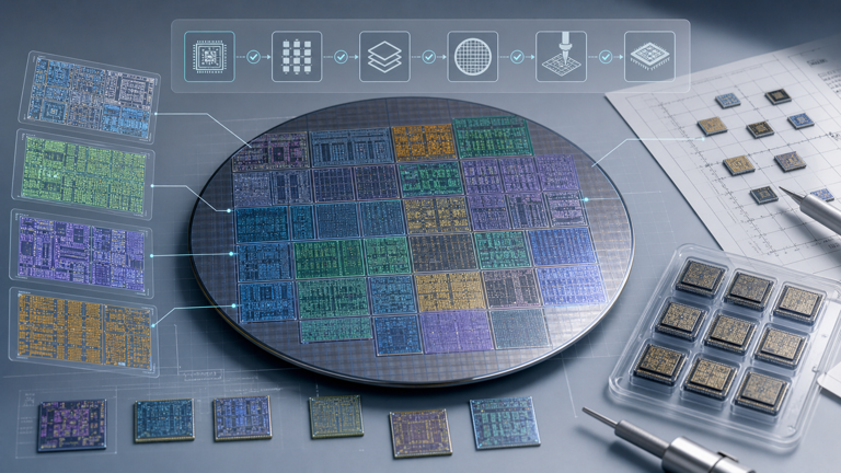
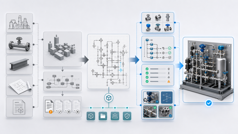
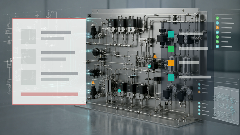
Browse by column
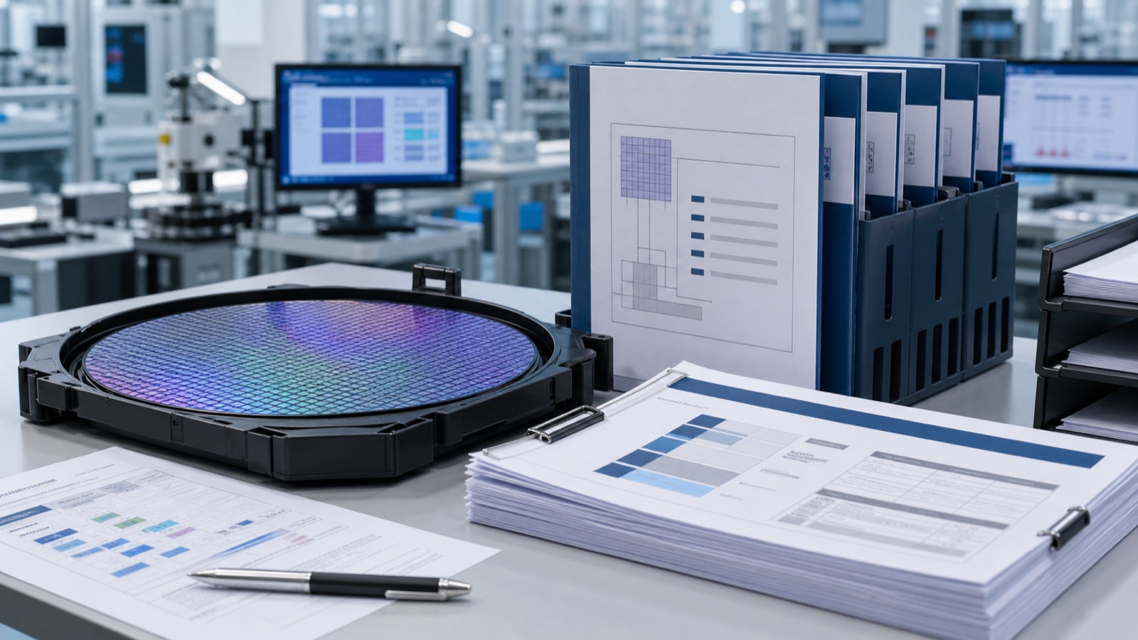 Company News
MST development and releases
Company updates, service launches, public resources and product release notes from Moore Solution Technology.
Industry Dynamics
Market and supply-chain notes
Practical notes on mature-node MPW, Asia access, equipment design trends and semiconductor supply-chain changes.
Technical Insights
Engineering guides and explainers
Focused technical articles on MPW flow, PDK/NDA/GDS, package/test, P&ID, BOM context and native SOLIDWORKS assembly.
 Product Updates
Tools and service updates
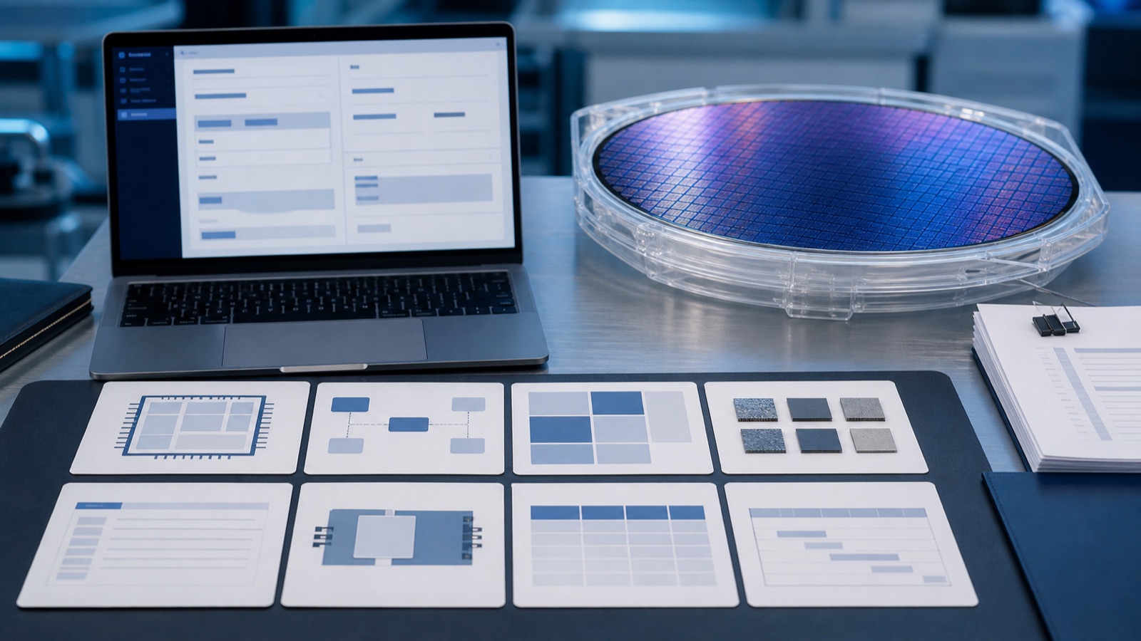
Updates for MST MPW tools, NeuroBox D review workflows and RFQ preparation resources.

MPW Packaging, Wafer Probe and Test: Specify Early
Why MPW RFQs should include packaging, wafer probe, sample count, test expectations and logistics before partner quotation.

Analog, BCD, High-voltage and RF MPW: Specialty-process Scoping
How to scope analog, mixed-signal, BCD, high-voltage and RF MPW requirements before NDA and partner confirmation.

MPW Readiness, PDK, NDA, Cost and Timeline Guide
A practical MPW guide covering readiness, PDK/NDA path, cost factors, shuttle windows, packaging and tapeout timeline.
Mature-node MPW: 0.35um to 40nm Process Scoping
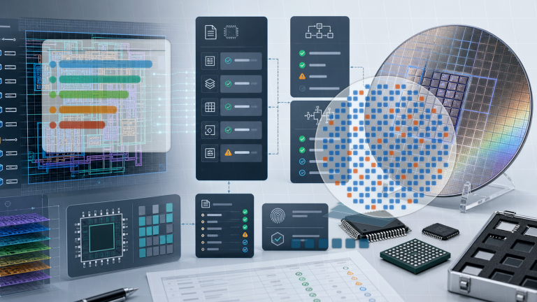
Scope mature-node MPW requirements across 0.35um to 40nm, including analog, mixed-signal, RF, BCD, high-voltage and eNVM process needs.
MPW RFQ Without GDS: What to Submit First
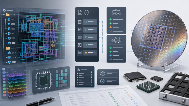
Start an MPW RFQ with outline requirements only: node, process family, die area, quantity and timeline. No GDS or design IP at intake.
MST Industrial Store Is Live: RFQ-Based Sourcing and Mature-Node MPW Tapeout Coordination
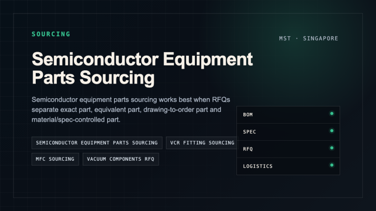
MST Industrial Store is live for overseas industrial buyers, with RFQ-based sourcing, drawing and BOM services, and mature-node MPW tapeout coordination.

How AI Lands in Semiconductor Fabs: A Practical Roadmap
Key TakeawayAI adoption in semiconductor fabs follows a clear 3-step pattern: start with VM, then add R2R, then EIP. Most failures happen from bad…

NeuroEnergy: AI-Driven Energy Management for Semiconductor Fabs
Key TakeawayNeuroEnergy is designed to reduce semiconductor fab energy costs by a targeted 8-15% through AI-driven optimization (design target). A typical fab consumes 50-100…

How Smart DOE Works for Semiconductor Equipment Commissioning
Key TakeawaySmart DOE uses Bayesian optimization and Latin hypercube sampling and is designed to reduce trial wafers by up to ~80% in modeled/offline scenarios…

NeuroBox E5200 Smart DOE for Semiconductor Trial-Wafer Planning
Key TakeawayNeuroBox E5200 is designed to help process teams evaluate Smart DOE trial-wafer planning before production use. In modeled and offline DOE scenarios, adaptive…
Related tools
MPW RFQ Pack Builder
Turn node, process family, die area, package/test assumptions, timeline and end-use context into a non-confidential first-screen brief.
P&IDP&ID Assembly Intake Checklist
Collect diagram quality, tag index, BOM, part library and rule context before asking whether a native SOLIDWORKS assembly pilot is realistic.
SourcingBOM RFQ Normalizer
Normalize messy BOM rows and expose missing manufacturer, quantity, drawing or description fields before supplier outreach.
Tell us what you need to manufacture, design or source.
Send a short brief for MPW tapeout and manufacturing coordination, a NeuroBox D P&ID-to-native-SOLIDWORKS review, or an engineering procurement RFQ.