I have a chip design. How do I get working first silicon?
Start by defining process fit, design readiness, the controlled PDK and data path, prototype quantity, package and test scope, then select a partner-confirmed run.

MST Singapore 是面向海外项目的非独家华虹(HHGrace)MPW 代理,承接产能询价、客户接入与项目协调。我们把非保密的节点、工艺、die、封装测试与目标时间整理成可提交 fab 评审的需求。实际产能、slot、排期、PDK 路径、报价与接单结果由 fab 逐项目确认。
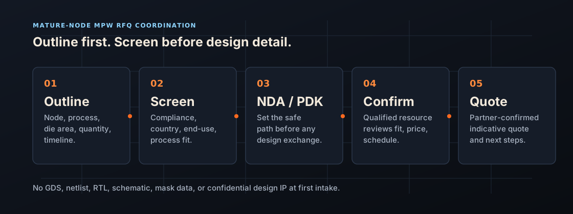
这是 MST Singapore 面向 2026 HHGrace(华虹)成熟节点 MPW RFQ 的公开排期筛查入口。它不是公开价格表,也不是保证 slot 的 shuttle 日历;具体 run 窗口、registration deadline、GDS/data-in deadline、PDK/NDA 路径、可用性和报价均在需求审核后逐案确认。
客户可以像查看公开 MPW 排期页一样使用这张表:先找到可能匹配的平台,再提交非保密首轮 brief,由 MST 检查当前排期窗口和报价路径。
| Node | Platform | Fit | 2026 status | What to send first | 下一步 |
|---|---|---|---|---|---|
| 90nm | 低功耗 BCD | 面向 BCD 与电源管理原型需求,电压等级、die 面积、封装/测试和样品需求需先评审。 | 2026 RFQ 筛查开放 | 节点目标、电压等级、die 预估、样品数量、封装/测试假设和目标季度。 | 开始适配筛选 → |
| 90nm | 嵌入式 eFlash | 面向嵌入式非易失存储和混合信号原型 RFQ,可先从非保密 brief 启动。 | 2026 RFQ 筛查开放 | 存储/工艺需求、die 预估、封装/测试假设、PDK/NDA 状态和目标季度。 | 开始适配筛选 → |
| 55nm | SiGe BiCMOS | 面向 RF、高速和混合信号原型筛查,需先确认工艺适配和封装/测试范围。 | 2026 RFQ 筛查开放 | RF/高速需求、粗略 die 尺寸、频段/用途背景、封装/测试假设和目标排期。 | 开始适配筛选 → |
| 55nm | 低功耗 BCD | 面向低功耗 BCD 与电源管理询价,需审核节点、电压、die 面积、排期和最终用途。 | 2026 RFQ 筛查开放 | 电压等级、应用背景、die 预估、目标样品和封装/测试假设。 | 开始适配筛选 → |
| 55nm | Logic / eFlash | 面向 logic 或 embedded-Flash 原型需求,MST 可在设计 IP 交换前准备可评审 RFQ。 | 2026 RFQ 筛查开放 | Logic/eFlash 需求、die 预估、封装/测试假设、PDK/NDA 状态和期望 tapeout 窗口。 | 开始适配筛选 → |
| 40nm | Logic / eFlash | 面向 40nm logic、低功耗或 embedded-Flash 原型路线,需伙伴准入和排期适配确认。 | 2026 RFQ 筛查开放 | 节点/工艺需求、die 预估、封装/测试假设、目标季度、国家/地区和最终用途背景。 | 开始适配筛选 → |
首次筛选只需要非保密信息,用于形成可评审需求;它不预留产能、不承诺 slot,也不替代 fab 确认。
目标节点或工艺类型、die 面积预估、样品需求、封装测试假设、目标季度、国家和最终用途。无需 GDS,也不要发送受保护设计 IP。
MST 核对工艺适配、缺失信息、NDA/PDK 路径、封装/晶圆测试/成品测试范围,以及需求是否可进入合作方评审。
适用路线、工艺资格、产能、slot、截止时间、PDK 获取、价格与接单结果,均由 fab 逐项目确认。
多数早期 MPW 访客还没有准备好提交完整 tapeout package。MST 提供四个低风险入口:比较入口路径、检查准备度、生成 no-GDS brief,或提交非保密 RFQ 由人工评审。
如果第一问题不是设计准备度,而是哪条路径、区域、资格门槛、NDA/PDK 路径和评审 owner 能处理请求,就先看入口地图。
打开入口地图 →使用 RFQ 包生成器,把节点、工艺类型、die 面积、样品目标、封装/测试假设、时间线和最终用途背景转成非保密首轮评审 brief。
生成 RFQ brief → 下载模板 ↓当您希望 MST 筛选工艺适配、封装/测试范围、NDA/PDK 路径、资格背景和合作方评审准备度时,提交非保密 brief。
发起非保密 MPW 需求咨询 →请提供节点范围、工艺类型、粗略 die 面积、样品目标、封装/测试假设、时间线和最终用途背景。MST 会在敏感设计数据移动前先筛选准备度。
以下为指示性工艺窗口。最终节点和工艺逐案由合格伙伴确认。
规划光罩、估算裸片数量和成本、检查 GDS 结构,并准备询价概要。运行并保存工具时,输入、所选原始附件和结果会发送至 MST 私密保存,供员工审核。MPW 询价表仍只接收非机密概要。
查看全部工具 →把多个项目打包进同一共享光罩,模拟晶圆 step-and-repeat,估算 gross/good dies 和各项目按面积分摊的成本。
打开规划器 →在浏览器检查顶层单元、裸片尺寸、图层和层级。点击“上传并检查”会将原始 GDS 和解析摘要发送至 MST 私密保存,供获授权员工查看。询价链接只携带高层级概要。
打开 GDS 检查器 →中立、带来源的 MPW 路线对比,覆盖 MOSIS、Europractice、Muse、IMEC 等选项,重点回答非美国/非欧盟团队实际能走哪条入口。资格、价格模型和 access gate 均按来源日期标注。
打开入口地图 →以下为示意性的非保密例子。它们说明 MST 首轮筛选需要什么范围,以及哪些内容应保留到 NDA 管控评审路径中。
客户提供: 客户提供目标节点范围、模拟/混合信号功能、粗略 die 面积、样品数量、封装偏好、测量目标和最终用途背景。
MST 返回: MST 返回缺失问题、可能的工艺族匹配、封装/probe/测试 checklist、NDA/PDK 路径说明和伙伴评审准备度。
后续受控路径: GDS、原理图、网表、PDK 文件和详细电路实现不进入公开入口,只在受控路径明确后再交换。
客户提供: 客户提供电压等级、器件选项假设、pad/封装方向、die 尺寸范围、安全或工业控制用途、目标样品和时间线。
MST 返回: MST 标记工艺适配不确定点、需要伙伴回答的问题、封装和可靠性假设、合规背景以及报价准备度缺口。
后续受控路径: 准确器件栈、专有电路细节、版图文件和伙伴特定设计规则,应等待 NDA/PDK 和合格技术评审。
客户提供: 客户以非保密方式提供 RF 频段或存储需求、可接受节点范围、粗略 die 面积、封装/测试假设和排期压力。
MST 返回: MST 区分公开规划问题和 NDA 后问题,并准备以可行性、入口路径和缺失假设为核心的伙伴评审包。
后续受控路径: 模型文件、IP block、专有版图、性能敏感原理图和工艺特定数据,应进入后续受控交换。
You may call it prototype tapeout, a shuttle run, a small engineering batch, packaged samples or simply “how do I get this chip made?” Choose the problem closest to yours; each route ends in an evidence checklist and a human-reviewed next step.
Start by defining process fit, design readiness, the controlled PDK and data path, prototype quantity, package and test scope, then select a partner-confirmed run.
A non-confidential readiness review can identify missing architecture, implementation, verification, signoff and commercial inputs before any protected design files move.
Yes. A first review can use node, process, die-area, sample, package, test and timing assumptions; price, slot and data acceptance still require formal confirmation.
Compare direct foundry access, an MPW service provider and a university or design-service route against your process, location, eligibility and support needs. Ask who holds the foundry relationship, arranges NDA/PDK access and owns the quotation and delivery scope. MST Singapore can prepare your non-confidential brief, identify missing inputs and coordinate the proposed partner-review path. Send the application, process target, approximate die area, sample need and timing first. Access and acceptance still require confirmation; a coordination service does not automatically include chip design or signoff.
Choose by voltage, embedded-memory, analog and RF needs, qualified IP, IO, die area, package, test and accessible ecosystem—not nominal node alone.
Map voltage devices, non-volatile memory, digital density, analog precision, IO and reliability needs first; a partner must then confirm the available process options.
Begin with a non-confidential requirement brief and entity and end-use context. NDA, PDK eligibility, technical fit and access are confirmed through the controlled partner path.
Country, customer type, end use, process family, schedule and data controls determine the realistic route; MST Singapore can structure the first review without public IP exchange.
Compare process fit, registration and data-in gates, minimum area, deliverables and readiness, then request the latest partner-confirmed window instead of relying on a static calendar.
The fastest route starts with a complete brief and a design close to the relevant signoff gate. Priority triage can reduce avoidable waiting, but no elapsed time is guaranteed.
Define whether you need wafers, loose die or packaged and tested units, then coordinate wafer run, probe, dicing, assembly, final test and logistics as separate confirmed scopes.
Recheck nearby nodes and process options, another operator or run, design readiness and whether an engineering or dedicated route better fits the business deadline.
There is no single MPW price: compare quotations for the same process option, area allocation and delivered sample scope. Ask whether each quote includes fabrication, masks where applicable, wafer probe, dicing, packaging, test development and final test, logistics and any taxes, and which items are separate. MST can prepare an initial quotation review from non-confidential process, die-area, sample-count, package/test and timing assumptions before final GDS. State whether you need bare dies, packaged parts or tested samples. An estimator is a planning aid; the formal quotation confirms price, inclusions, exclusions, validity and availability.
Die area can affect shared-wafer allocation while deliverable quantity, yield assumptions, package choice, probe and final-test coverage change downstream scope and cost.
Foundry-specific signoff, final data acceptance, run registration, mask and wafer execution, probe, dicing, packaging, final test, logistics and bring-up can still remain.
Include country and end use, target node or range, process family, die estimate, samples, package and test assumptions, timing and NDA or PDK status—without design IP.
The foundry, probe house, OSAT, test house, logistics provider and customer may own different steps. The quotation must name the deliverable and each confirmed owner.
Start with the intended evidence and sample form. Test coverage, fixtures, ATE programs, characterization and reliability plans are separate scopes that need named ownership.
Define bring-up evidence, failure isolation, change scope, reusable masks or layers if applicable, verification closure and the decision gate between another MPW and a dedicated run.
Choose a foundry or MPW service route that can confirm both prototype access and a later production option for your specific process. MST Singapore can prepare a non-confidential brief and coordinate partner review: include expected annual volume, product lifetime, qualification needs, package/test scope and target timing from the start. Use first-silicon measurements to decide on another prototype or an engineering lot, then agree the qualification, test and production plan with named owners. A successful MPW run does not establish a production supply agreement. Eligibility, capacity, quotation and any long-term supply commitment require separate written confirmation from the responsible partners.
Public first contact is non-confidential. Do not send GDS, OASIS, RTL, netlists, schematics, PDK files or proprietary IP until the controlled NDA/data path is confirmed.
工程团队和采购团队在提交简报前最常问的问题。
先提交非保密 brief,说明节点/工艺适配、目标排期、首片硅验证、封装/测试、样品处理或重新流片需求。MST 将需求转入审核;可行性、可用性、时间和报价均逐案确认。