
Technical Insights
Focused technical articles on MPW flow, PDK/NDA/GDS, package/test, P&ID, BOM context and native SOLIDWORKS assembly.
Technical Insights
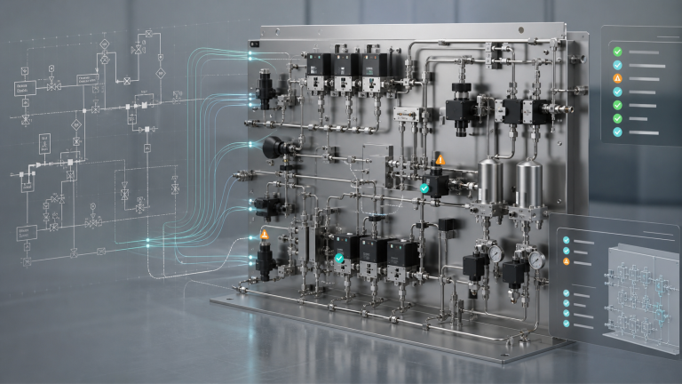
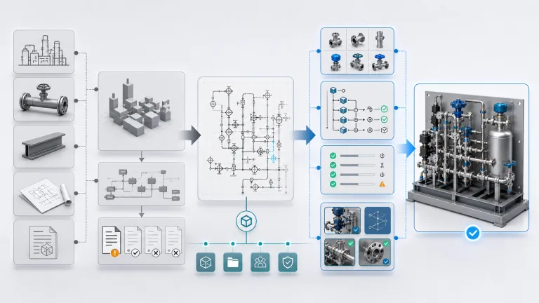
AI P&ID to SOLIDWORKS for Gas Panel Design Automation
Gas panels and gas boxes are strong candidates for P&ID-to-native-assembly automation because they combine repeated patterns, strict rules, BOM pressure and frequent variants.
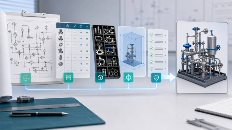
What Inputs Are Needed for P&ID to SOLIDWORKS Assembly Generation?
A practical checklist for starting a P&ID-to-native-SOLIDWORKS review: diagram quality, part library, BOM fields, spatial envelope, rulepack and output expectations.
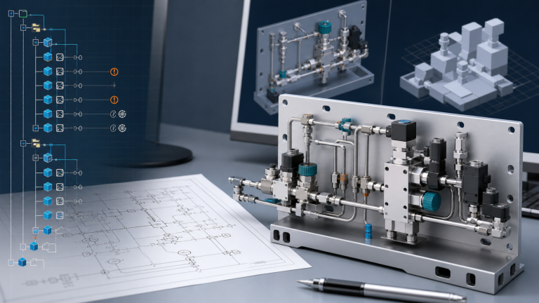
P&ID to SOLIDWORKS Assembly: Feature Tree vs STEP Export
Why native SOLIDWORKS assemblies with feature tree, mates, BOM context and reusable parts are more useful than neutral geometry export for P&ID-driven equipment design.
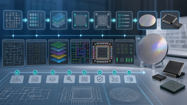
What Information Is Needed for an MPW RFQ?
A good MPW RFQ is not a data dump. It is a clear, non-confidential summary that lets the coordination team screen process fit, readiness,…
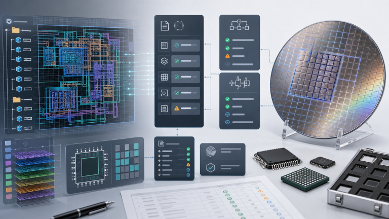
Can You Start an MPW RFQ Without GDS?
A first MPW RFQ should protect design IP. Start with non-confidential requirements, then move to NDA, PDK and partner-confirmed review before any design detail…
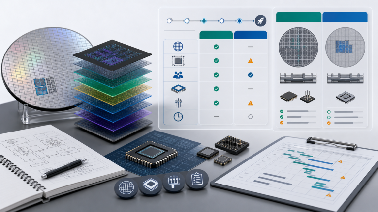
MPW vs Pilot Wafer vs Full Mask: Which Route Fits Your Chip?
A practical decision guide to shared MPW, pilot wafer or engineering lots, and dedicated full-mask production—covering maturity, schedule, splits, samples, package, test and scale-up.
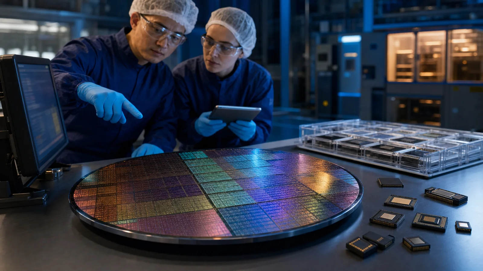
What Is MPW in Semiconductor? Tapeout to First Silicon
MPW combines multiple chip designs on a shared wafer run. Learn when it fits, what affects cost and schedule, and what to prepare before…
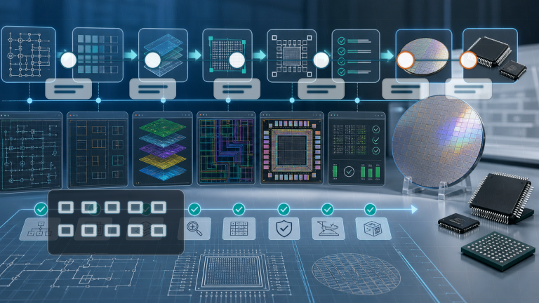
MPW Packaging and Test Tutorial: Plan Your First Silicon
Plan MPW wafer probe, die handling, packaging and first-silicon testing with a worked sample allocation and a die-to-package checklist.
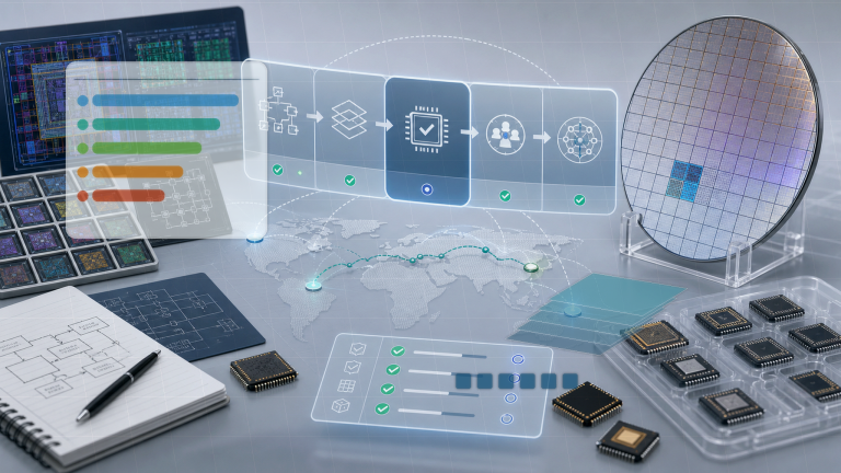
Analog, BCD, High-voltage and RF MPW: Specialty-process Scoping
How to scope analog, mixed-signal, BCD, high-voltage and RF MPW requirements before NDA and partner confirmation.
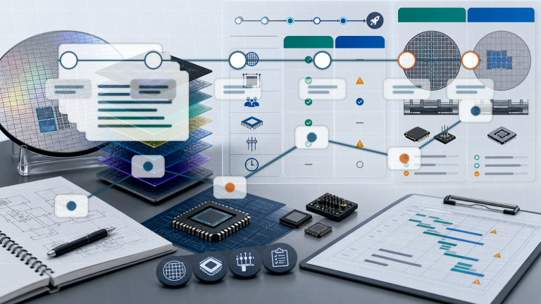
MPW Readiness, PDK, NDA, Cost and Timeline Guide
A practical MPW guide covering readiness, PDK/NDA path, cost factors, shuttle windows, packaging and tapeout timeline.
Tell us what you need to manufacture, design or source.
Send a short brief for MPW tapeout and manufacturing coordination, a NeuroBox D P&ID-to-native-SOLIDWORKS review, or an engineering procurement RFQ.