How Much Does Chip Tapeout Cost? MPW vs Full Mask Cost Drivers
Chip tapeout cost depends on node, process family, die area, MPW eligibility, package, test and schedule. Use this guide before asking for a quote.
- →Why tapeout cost varies so much
- →MPW cost vs full mask cost
- →What a startup should prepare before asking for price
- →FAQ
Answer block: Chip tapeout cost is driven by node, mask strategy, die area, shuttle eligibility, packaging, wafer probe, test, engineering work and schedule risk. MPW can make prototype silicon more accessible because resources are shared, while full mask usually gives stronger control for mature designs. A useful cost discussion starts with non-confidential scope, not with GDS.
“How much does a tapeout cost?” is one of the most common questions from founders, researchers and hardware teams. The honest answer is that there is no single public price that applies to every route. Public shuttle pages and access programs show that the market has many routes, but every serious quote depends on design scope, process fit and commercial eligibility.
Why tapeout cost varies so much
Two chips at the same nominal node can have very different economics. A small digital test chip, an RF front end, a high-voltage mixed-signal ASIC and a MEMS-adjacent design do not create the same partner review, design-rule, package or test burden.
The biggest cost drivers are:
- Node and process family: mature CMOS, analog, BCD, RF, high-voltage and embedded memory options have different access paths.
- Mask route: shared MPW, engineering run or full mask.
- Die area: larger die consume more shared real estate and can affect fit.
- Packaging and test: wafer probe, dicing, package selection, sample count and test program readiness all matter.
- Schedule: a team that can wait for a shuttle window has different options from a team with a fixed customer deadline.
- Design readiness: DRC/LVS, pad ring, IO, PDK and reliability assumptions shape partner review.
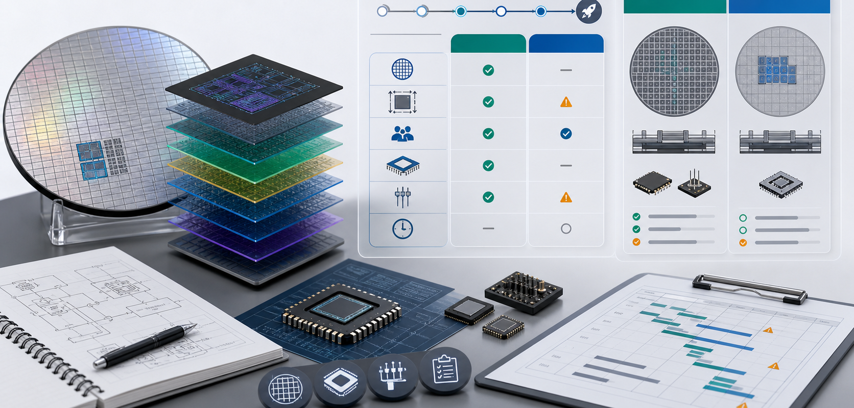
MPW cost vs full mask cost
MPW is often the first route to consider for prototype silicon because it shares wafer or mask resources across projects. Full mask is usually considered when the design is mature, the quantity target is clearer, or the program needs dedicated control.
| Cost question | MPW | Full mask |
|---|---|---|
| Initial prototype access | Usually more accessible | Usually higher commitment |
| Schedule flexibility | Bound by shuttle windows | More route control once committed |
| Sample quantity | Prototype oriented | Better for larger program planning |
| Change after first silicon | Often expected | More expensive if the design is not stable |
What a startup should prepare before asking for price
A good first request does not need confidential layout. It needs enough structure for a partner to judge fit:
- Target node or acceptable node range.
- Process type and special devices required.
- Approximate die size and number of samples.
- Package and test expectations.
- Whether PDK access, NDA and EDA flow are already in place.
- Target shuttle window or first-silicon date.
If those fields are missing, the first answer will usually be a scoping request, not a quote. Use the MPW Cost & Dies Estimator and the Reticle & Wafer Planner for non-confidential planning before sending an RFQ.
FAQ
Can MST give an instant MPW price?
No. MST can provide an indicative screening read and coordinate partner-confirmed RFQs, but route, eligibility, package and test assumptions must be reviewed.
Is 180nm always cheaper than 65nm?
Not always in a simple way. Mature-node access, process family, shuttle availability, die area and package/test scope all affect economics.
Should I choose MPW only because it appears cheaper?
No. Choose MPW when the goal is prototype silicon and learning. Choose full mask when the design and program need dedicated control.
For route comparison, start with the MPW shuttle guide and MST’s mature-node MPW coordination page.
准备定义您的项目?
发送节点、工艺类型、芯片面积、数量和时间线 - 不包含设计 IP。我们筛选后对接合格伙伴,并返回伙伴确认后的下一步。