
新闻与洞察
技术洞察
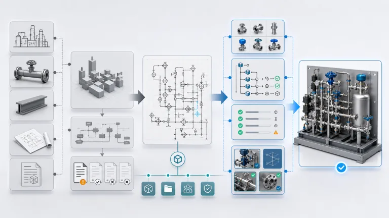
聚焦 MPW 流程、PDK/NDA/GDS、封装测试、P&ID、BOM 上下文和原生 SOLIDWORKS 装配。
技术洞察
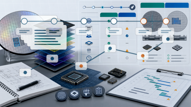
MPW Readiness, PDK, NDA, Cost and Timeline Guide
A practical MPW guide covering readiness, PDK/NDA path, cost factors, shuttle windows, packaging and tapeout timeline.
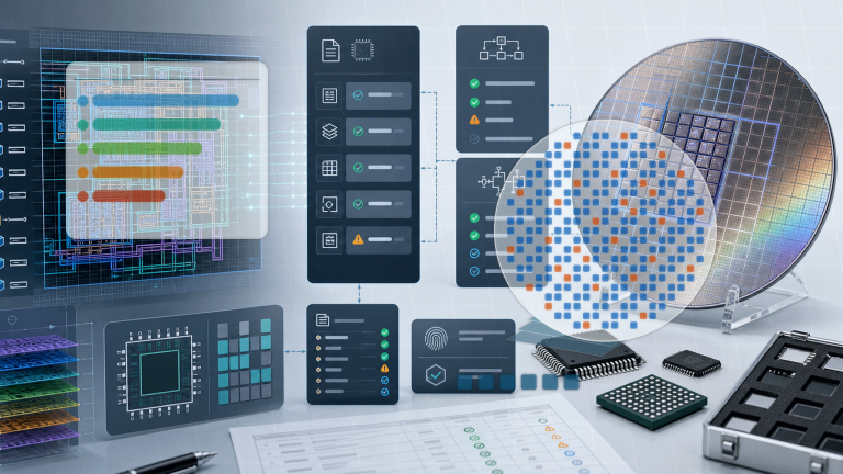
Mature-node MPW: 0.35um to 40nm Process Scoping
Scope mature-node MPW requirements across 0.35um to 40nm, including analog, mixed-signal, RF, BCD, high-voltage and eNVM process needs.
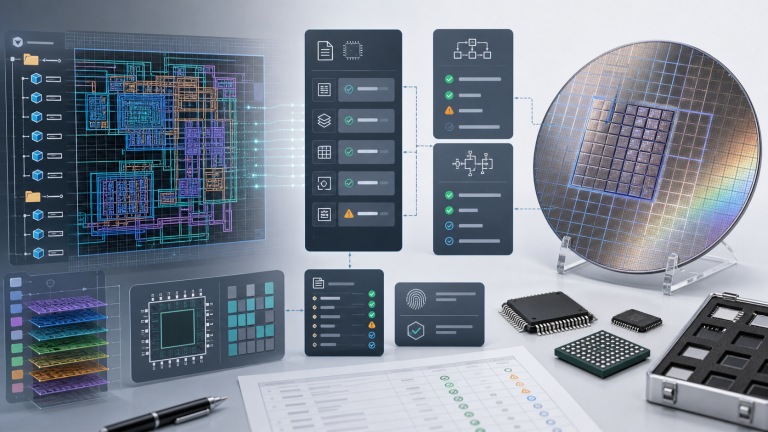
MPW RFQ Without GDS: What to Submit First
Start an MPW RFQ with outline requirements only: node, process family, die area, quantity and timeline. No GDS or design IP at intake.
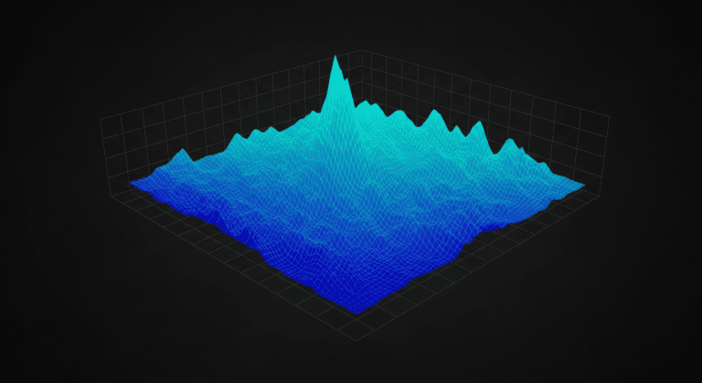
How Smart DOE Works for Semiconductor Equipment Commissioning
Key TakeawaySmart DOE uses Bayesian optimization and Latin hypercube sampling and is designed to reduce trial wafers by up to ~80% in modeled/offline scenarios…
从您的需求开始
告诉我们你要制造、设计或采购什么。
提交一段简短说明:MPW 流片与制造协调、NeuroBox D P&ID-to-3D 评审,或工程采购 RFQ。