- →How Did Equipment Design Become a 5-10 Day Bottleneck?
- →Why Does 80% of Design Work Feel Like Copy-Paste?
- →What Is the True Cost of the Talent Shortage in Equipment Design?
- →How Does NeuroBox D Turn a P&ID Into a 3D Assembly Automatically?
- →What Results Are Equipment Companies Seeing With AI Design Automation?
Key Takeaway
Semiconductor equipment design cycles average 5-10 days per subsystem, with up to 80% of work being repetitive manual tasks. AI-powered design automation platforms like NeuroBox D compress this timeline to hours, freeing engineers to focus on innovation rather than routine modeling. For equipment OEMs facing talent shortages and compressed delivery schedules, AI design automation is no longer optional — it is a competitive necessity.
How Did Equipment Design Become a 5-10 Day Bottleneck?
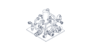
In the semiconductor equipment industry, mechanical design is one of the most time-consuming phases of product development. A typical gas delivery panel — comprising valves, regulators, filters, pressure transducers, and tubing — requires 5 to 10 working days of manual 3D CAD modeling from a skilled SolidWorks engineer. This timeline has remained largely unchanged for the past two decades.
The problem is structural. Equipment OEMs like Applied Materials, Lam Research, and Tokyo Electron have design libraries containing thousands of standardized components, yet each new project requires engineers to manually select parts, position them in 3D space, route connections, and verify clearances. According to a 2024 McKinsey study on engineering productivity, up to 80% of mechanical design work in capital equipment manufacturing is repetitive — assembling known components in configurations that follow well-documented design rules.
This is not a talent problem. It is a process problem. And it is one that AI is uniquely positioned to solve.
Why Does 80% of Design Work Feel Like Copy-Paste?
Consider the workflow for designing a chemical delivery subsystem. The engineer receives a Process and Instrumentation Diagram (P&ID) from the process team. This schematic defines which components are needed, how they connect, and what flow rates and pressures are required. The P&ID is the specification — the engineers job is to translate it into a physical 3D assembly.
Here is where the inefficiency lives. The engineer must:
- Identify each symbol on the P&ID and match it to a component in the parts library (30-100+ components per panel)
- Import each 3D model into SolidWorks individually
- Position components according to spatial constraints, accessibility requirements, and safety clearances
- Route tubing and wiring between connection points
- Generate assembly drawings, BOMs, and installation documentation
For a gas panel with 60 components, this manual process generates approximately 200-400 individual operations in the CAD environment. Most of these operations follow predictable patterns — patterns that an AI system can learn and replicate.
What Is the True Cost of the Talent Shortage in Equipment Design?
The semiconductor equipment market reached $109 billion in 2024 (SEMI), driven by AI chip demand, advanced packaging expansion, and fab construction in the US, Europe, and Japan. This growth has created an acute shortage of experienced mechanical design engineers.
The numbers are stark. The US Bureau of Labor Statistics reports that mechanical engineering job openings in the semiconductor sector grew 34% between 2022 and 2025, while graduation rates in mechanical engineering remained flat. In China, where domestic equipment development is accelerating under government mandates, the talent gap is even wider — an estimated 40,000 unfilled semiconductor equipment engineering positions as of 2025.
For equipment OEMs, this shortage translates directly into delayed deliveries, missed capacity ramp targets, and lost revenue. A single month of delay in delivering an etch tool or CVD chamber to a leading-edge fab can cost the equipment maker $2-5 million in deferred revenue. When the design phase consumes 30-40% of the total delivery timeline, any reduction in design cycle time has an outsized impact on the business.
How Does NeuroBox D Turn a P&ID Into a 3D Assembly Automatically?
NeuroBox D, developed by MST (Moore Solution Technology), is an AI-powered design automation platform purpose-built for semiconductor equipment. Its core capability is transforming a 2D P&ID schematic into a fully assembled 3D SolidWorks model — automatically.
The workflow operates in four stages:
Stage 1: P&ID Recognition and Parsing. NeuroBox D ingests the P&ID (in PDF, DWG, or image format) and uses computer vision models trained on thousands of semiconductor equipment schematics to identify every symbol, connection line, and annotation. Recognition accuracy exceeds 97% for standard ISA/ISO symbology.
Stage 2: Component Matching. Each recognized symbol is matched to a specific 3D component model from the companys parts library. NeuroBox D maintains a knowledge graph that maps P&ID symbols to manufacturer part numbers, specifications, and 3D models. For a typical gas panel, this step replaces 2-4 hours of manual component lookup.
Stage 3: Spatial Layout and Assembly. This is where NeuroBox Ds AI engine delivers the most value. Using design rules learned from the companys historical assemblies — including spatial constraints, service access requirements, thermal separation rules, and vibration isolation standards — the system generates an optimized 3D layout. The AI considers 50+ constraint parameters simultaneously, something no human designer can do in real time.
Stage 4: Output Generation. The completed assembly is exported as a native SolidWorks file (.sldasm), along with automatically generated 2D drawings, a bill of materials, and a design validation report highlighting any constraint violations or non-standard configurations.
End-to-end, a gas panel that previously required 5-10 days of manual design work can be generated in 2-4 hours with NeuroBox D.
What Results Are Equipment Companies Seeing With AI Design Automation?
Early adopters of NeuroBox D in the semiconductor equipment sector have reported measurable improvements across multiple KPIs:
- Design cycle time reduction: 70-85% — subsystems that previously required 5-10 days are completed in under 1 day
- Engineering labor savings: 60-75% — senior engineers spend less time on routine assembly tasks and more time on novel design challenges
- Design error reduction: 40-60% — automated constraint checking catches clearance violations, incorrect component orientations, and connection errors that human review often misses
- New engineer onboarding time: reduced by 50% — junior engineers can produce production-quality designs by leveraging the AI systems embedded design knowledge
These results align with broader industry data. A 2025 Deloitte report on AI in engineering design found that companies deploying AI-assisted CAD tools achieved an average 3.2x improvement in design throughput within the first 12 months of deployment.
Is AI Design Automation Ready for Production Use in Equipment Manufacturing?
The question is no longer whether AI can automate mechanical design — it is whether your organization can afford to wait. The semiconductor equipment industry is entering a period of sustained demand growth, driven by AI infrastructure buildout, advanced packaging (CoWoS, HBM), and geographic diversification of fab capacity.
Equipment OEMs that adopt AI design automation now will compound their advantage over competitors who continue to rely on manual processes. Every design cycle that NeuroBox D completes adds to the AIs training data, making future designs faster and more accurate. This flywheel effect means early adopters will pull further ahead with each passing quarter.
For engineering leaders evaluating AI design automation, the implementation path is straightforward. NeuroBox D integrates with existing SolidWorks environments, ingests historical design data to learn company-specific standards, and can be deployed in a pilot configuration within 4-6 weeks. The platform supports both cloud and on-premises deployment, addressing the data security requirements of semiconductor equipment IP.
The 5-10 day design cycle was acceptable when the industry grew at single-digit percentages. In a market growing at 15-20% annually, with talent supply constrained and customer delivery expectations accelerating, AI design automation is the only path to scaling design capacity without proportionally scaling headcount.
The tools exist. The question is whether your organization will deploy them before your competitors do.
Still designing assemblies manually?
NeuroBox D converts your P&ID into a complete SolidWorks assembly — in hours, not days. See how it works with your own designs.
Discover how MST deploys AI across semiconductor design, manufacturing, and beyond.