- →The a16z Framework: What Makes Enterprise AI Adoption Work
- →The Harvey Precedent: Why "Hard Markets" Can Produce Outsized Returns
- →Semiconductor Equipment AI: The Same Playbook
- →The Window Is Open — But Not Forever
- →Implications for Equipment OEMs and Fab Operators
Key Takeaways
Source: Moore Solution Technology (mst-sg.com)
a16z just published the most rigorous enterprise AI adoption data we have seen. Their report tracks spending patterns across the Fortune 500 and Global 2000, maps revenue trajectories of leading AI startups, and identifies which industries are adopting fastest — and which are still waiting on the sidelines.
See how AI transforms semiconductor design and manufacturing — from the equipment up.
Choose how you'd like to connect:
One conclusion stands out: the next wave of AI value creation will come from industries that are “hard” — those with real-world operations, domain expertise requirements, and long sales cycles. That is exactly where we have placed our bet.
As a founder building AI software for semiconductor equipment, I have spent the past three years navigating every obstacle the a16z report describes: long procurement cycles, risk-averse buyers, real-time operational requirements, and the need for deep process knowledge before you can write a single line of model code. Reading their data felt like reading a validation of our thesis.
This article is my analysis of what the a16z enterprise AI report means for the semiconductor equipment industry — and why I believe this sector is about to produce its own “Harvey moment.”
The a16z Framework: What Makes Enterprise AI Adoption Work
Let us start with the data. a16z’s report reveals several patterns that should inform every vertical AI strategy:
The market is real and growing fast. 29% of Fortune 500 companies are now paying customers of top AI startups. 19% of the Global 2000 have deployed enterprise AI solutions in production. These are not pilot programs or innovation lab experiments — these are paid, deployed, operational systems generating measurable ROI.
Revenue concentration follows a clear pattern. The fastest-growing AI revenue categories are coding assistants, customer service automation, and AI-powered search. What do these categories have in common? Five characteristics that make AI adoption frictionless:
- Text-heavy workflows — The core work product is language-based, which plays directly to LLM strengths
- Repetitive task structures — High-volume, pattern-recognizable activities where automation delivers immediate time savings
- Verifiable outputs — You can check whether the code compiles, whether the customer query was resolved, whether the search result was relevant
- Low regulatory barriers — No FDA approval, no safety certification, no multi-year validation processes
- Individual user adoption — A single developer or support agent can start using the tool without enterprise-wide procurement
This is why coding (GitHub Copilot, Cursor) and customer service (Intercom, Zendesk AI) dominate today’s AI revenue charts. The adoption friction is minimal. A developer installs a plugin and starts coding faster by lunchtime. A support team enables AI responses and sees ticket resolution times drop within a week.
But here is what most people miss in the a16z data: the report explicitly identifies a second category of industries — those characterized by “real-world operations, complex relationships, regulatory thresholds, and hard-to-verify results” — where AI adoption is slower today but where the eventual value capture may be far larger. These are the industries where software alone cannot solve the problem. You need domain expertise embedded in the product itself.
This is where the Harvey precedent becomes instructive.
The Harvey Precedent: Why “Hard Markets” Can Produce Outsized Returns
Before Harvey, legal technology was considered a graveyard for startups.
The conventional wisdom was well-established: law firms are conservative, partners resist change, procurement takes forever, data is sensitive and siloed, and the profession has a deep cultural aversion to automation. For decades, legal tech companies struggled to grow beyond modest revenue bases. The industry was “too hard” for software.
Harvey proved that analysis catastrophically wrong.
In roughly three years, Harvey reached approximately $200M in annual recurring revenue — a growth trajectory that rivals consumer SaaS companies, achieved in an industry that was supposed to be impervious to disruption. How?
The copilot-first strategy. Harvey did not try to replace lawyers. It positioned itself as an AI assistant that makes lawyers faster, more thorough, and more consistent. This is critical. In domains where practitioners have deep expertise and professional pride, the “replacement” narrative is toxic. The “augmentation” narrative is magnetic. Harvey’s early product was a research copilot — it helped associates find relevant precedents, draft memos, and review contracts faster. It made good lawyers better instead of trying to eliminate them.
Deep workflow integration. Harvey did not build a generic chatbot that happened to know some law. It integrated into the actual workflows lawyers use every day — document review, due diligence, contract analysis, legal research. The AI was embedded in the work, not adjacent to it. This made adoption natural rather than disruptive.
Domain-specific model tuning. Harvey invested heavily in training and fine-tuning models on legal corpora — case law, statutes, regulatory filings, firm-specific precedents. The result was an AI that spoke the language of law, understood legal reasoning patterns, and could produce outputs that met the profession’s quality standards. A generic GPT wrapper could not have achieved this.
Trust through verifiability. Legal work has a built-in verification mechanism: citations. Harvey’s outputs include references to specific cases, statutes, and documents. A lawyer can check the AI’s work. This verifiability was essential for adoption in a profession where errors carry malpractice risk.
The Harvey lesson is not that legal AI is special. The lesson is that “hard” industries can produce the fastest-growing AI companies precisely because the barriers to entry keep competition out. Once you crack the code — once you build the domain expertise, the workflow integration, and the trust mechanisms — you have a moat that generic AI tools cannot cross.
a16z says this explicitly in their report: “Go find sectors where model capability is improving fast but no revenue breakout company exists yet.”
That brings us to semiconductor equipment.
Semiconductor Equipment AI: The Same Playbook
The parallels between legal AI three years ago and semiconductor equipment AI today are striking. Both industries share the same structural characteristics that initially deter AI startups — and the same characteristics that create massive opportunities for those who persist.
| Factor | Legal AI (Harvey) | Semiconductor Equipment AI (MST) |
|---|---|---|
| Industry perception | “Law firms don’t buy software” | “Fabs and equipment OEMs are too conservative for AI” |
| Domain expertise barrier | Must understand legal reasoning, case law, regulatory frameworks | Must understand plasma physics, process chemistry, equipment mechanics, SEMI standards |
| Data sensitivity | Client-privileged information, confidential deals | Process recipes (trade secrets), yield data, equipment IP |
| Buyer conservatism | Partners bill $1,000+/hr, resist changing proven workflows | Equipment worth $5–50M per tool, zero tolerance for unplanned downtime |
| Sales cycle | 6–12 months, committee-driven | 6–18 months, requires on-site PoC and validation |
| Verification mechanism | Case citations, statutory references (checkable) | Wafer metrology data, SPC charts, yield metrics (measurable) |
| Entry strategy | Copilot for legal research → expand to contract review, due diligence | Copilot for equipment commissioning → expand to VM, R2R, predictive maintenance |
| Moat once established | Firm-specific precedent data, trained on proprietary workflows | Equipment-specific process models, proprietary sensor data, validated on production wafers |
| Cost of failure | Malpractice liability, reputational damage | Scrapped wafers ($2K–50K each), tool downtime ($10K–100K/hr) |
| Market size | Global legal services: ~$1T | Global semiconductor equipment + manufacturing: $600B+ |
The structural similarity is not coincidental. It reflects a deeper truth about vertical AI: the same factors that make an industry “hard to sell to” also make it incredibly defensible once you are inside.
Consider the domain expertise barrier. Harvey needed to build a team that understood how lawyers actually work — not the Hollywood version, but the mundane reality of document review, citation checking, and regulatory compliance. Similarly, building AI for semiconductor equipment requires understanding not just machine learning, but plasma physics, thin-film deposition chemistry, CMP slurry dynamics, and the SEMI communication standards (GEM/SECS) that govern how equipment talks to factory systems.
This dual requirement — AI expertise plus deep domain knowledge — is what a16z calls the “domain expert moat.” It is the reason generic AI platforms consistently fail in these markets. You cannot fine-tune GPT-4 on a few semiconductor textbooks and expect it to optimize an etch recipe. The knowledge required is tacit, experiential, and deeply embedded in years of working with actual equipment on actual production lines.
Consider the copilot entry strategy. Harvey did not walk into law firms and say “our AI will replace your associates.” That would have triggered an immune response. Instead, Harvey said “our AI will make your associates 3x faster at legal research.” The associate still does the work. The partner still reviews it. The AI simply removes the drudgery and accelerates the process.
We follow the identical playbook. Our entry point at MST is equipment commissioning — the process of bringing a new semiconductor tool from installation to production-qualified status. Today, this process takes weeks of manual recipe tuning, hundreds of test wafers, and the undivided attention of senior process engineers. Our NeuroBox platform acts as a copilot for commissioning engineers: it analyzes sensor data in real-time, recommends recipe adjustments based on historical patterns across similar tools, and reduces the number of test wafers needed by up to 80%.
The engineer still makes every decision. The AI makes the engineer faster, more consistent, and less dependent on individual heroics. This is the copilot model — and it works in conservative industries because it respects the expertise of the people it serves.
The Window Is Open — But Not Forever
The a16z report contains an explicit call to action for builders that should alarm anyone not yet moving in this space:
“Go find sectors where model capability is improving fast but no revenue breakout company exists yet.”
Semiconductor equipment AI fits this description precisely. Let us examine why the window is open right now — and why it will not stay open indefinitely.
The market is massive and underserved
Global semiconductor manufacturing is a $600B+ industry. Equipment spending alone exceeded $100B in 2024. Yet AI penetration in semiconductor equipment operations remains below 5%. The vast majority of process optimization, fault detection, and equipment commissioning is still done manually or with rule-based systems designed in the 1990s.
Compare this to the industries that a16z identifies as “most active” in AI adoption: technology, legal, and healthcare. These industries have dozens of well-funded AI startups competing for market share. Semiconductor equipment has almost none. The ratio of market opportunity to startup activity is wildly skewed.
Model capability has crossed the production threshold
Two years ago, deploying AI in a semiconductor fab required custom model development for every tool, every process, and every recipe. The engineering cost was prohibitive for all but the largest foundries. Today, foundation models and transfer learning techniques have fundamentally changed the equation.
We can now train a virtual metrology model on 15 wafers of data from a new tool — transferring knowledge from models trained on similar tools at other sites — and achieve production-grade accuracy within days. Run-to-run control algorithms that once required months of statistical modeling can now be deployed in weeks using physics-informed neural networks. The models are ready. The infrastructure is ready. What is missing is the domain-specific company that packages this capability into a product that semiconductor engineers can actually use.
First-mover advantage in vertical AI is extreme
This is perhaps the most important insight from the a16z framework. In horizontal AI (chatbots, coding assistants, search), multiple well-funded competitors can coexist because the market is enormous and switching costs are low. In vertical AI, the dynamics are completely different.
When you deploy AI on a semiconductor tool, the model trains on that specific tool’s data. Over time, the model accumulates operational knowledge — failure modes, drift patterns, recipe sensitivities — that is unique to that equipment. Ripping out the AI system and replacing it with a competitor’s product means losing all of that accumulated knowledge and starting the learning process from scratch. The switching cost is not financial; it is operational.
This creates a powerful “land and expand” dynamic. The first AI vendor to deploy on a tool has a structural advantage that compounds over time. Each month of operation makes the model more valuable and the switching cost higher. This is why Harvey’s early penetration of top law firms was so strategically important — and why the race to deploy AI on semiconductor equipment tools is a race that rewards speed above almost everything else.
The competitive landscape is thin
Look at who is building AI for semiconductor equipment today. The large equipment OEMs (Applied Materials, Lam Research, Tokyo Electron, ASML) are investing in AI internally, but their efforts are focused on their own tool platforms and their own process recipes. They are not building horizontal AI platforms that work across vendors and across process types.
The large industrial AI platforms (C3.ai, Palantir, Siemens MindSphere) have generic capabilities but lack the semiconductor-specific domain knowledge. They can build dashboards and run anomaly detection algorithms, but they cannot tell an etch engineer why the RF matching network impedance is drifting or recommend a specific recipe adjustment for a CVD chamber seasoning issue.
The academic and research community has published thousands of papers on semiconductor AI, but the translation from research to production-deployable software remains largely undone.
The window exists because no one has yet built the Harvey of semiconductor equipment AI — a vertically integrated, domain-expert AI company purpose-built for this industry. That is the opportunity.
Implications for Equipment OEMs and Fab Operators
The a16z data is not just relevant for AI startups. It carries urgent implications for the two groups that constitute the semiconductor equipment ecosystem: the OEMs that build the tools and the fabs that operate them.
For equipment OEMs: AI is becoming a competitive requirement
The a16z report documents a clear pattern: in every industry where AI adoption accelerates, the vendors who embed AI into their products capture disproportionate market share. This is happening in developer tools (GitHub vs. competitors), in customer service platforms (Intercom vs. legacy helpdesks), and in legal services (Harvey vs. traditional legal research tools).
The same dynamic will play out in semiconductor equipment. As leading fabs begin to require AI-ready equipment — tools that can expose real-time sensor data, support automated recipe optimization, and integrate with factory-wide AI systems — OEMs without AI capabilities will find themselves at a procurement disadvantage.
This does not mean every OEM needs to build AI in-house. Harvey did not require law firms to build their own AI. It provided the AI layer that law firms could deploy on top of their existing workflows. The analog for equipment OEMs is clear: partner with specialized AI companies that can add an intelligent software layer to your hardware platform, rather than trying to build AI competency from scratch in an organization optimized for mechanical and electrical engineering.
The OEMs that move first will have a meaningful advantage. When your equipment comes with AI-powered commissioning that reduces setup time by 60%, AI-driven predictive maintenance that cuts unplanned downtime by 40%, and virtual metrology that eliminates 70% of physical measurements — that is not a feature. That is a reason for a fab to choose your tool over the competition.
For fabs: early AI adopters will have structural cost advantages
The a16z data on Fortune 500 AI adoption reveals something important: early adopters are not experimenting with AI. They are deploying it at scale and realizing compounding cost advantages that late adopters cannot easily replicate.
In semiconductor manufacturing, these advantages are concrete and quantifiable:
- Virtual metrology reduces physical measurement steps by 50–80%, directly increasing tool utilization and throughput
- Run-to-run control reduces process variation by 30–50%, translating directly to yield improvement
- Smart commissioning reduces equipment qualification time by 40–60%, accelerating time-to-revenue for new capacity
- Predictive maintenance reduces unplanned downtime by 25–40%, improving overall equipment effectiveness (OEE)
- Fault detection and classification catches excursions 10–100x faster than SPC, preventing cascading yield loss
Each of these improvements compounds. A fab that deploys AI across commissioning, production monitoring, and maintenance creates a structural cost advantage that widens with every quarter of operation. The AI models get better. The operational data accumulates. The cost gap between AI-enabled and AI-absent operations grows.
This is the same dynamic a16z observes in enterprise software adoption: the gap between leaders and laggards is not narrowing. It is widening.
The CHIPS Act is accelerating the timeline
The global push to diversify semiconductor manufacturing — the U.S. CHIPS Act, the European Chips Act, Japan’s semiconductor investment program, India’s fab incentives — is creating a wave of new fab construction and equipment procurement. Tens of billions of dollars are flowing into greenfield and brownfield semiconductor facilities.
This matters for AI adoption in two ways:
First, new fabs have no legacy systems to protect. They can design their manufacturing execution systems, data infrastructure, and process control architectures with AI as a first-class requirement rather than a retrofit. This eliminates the largest adoption barrier that existing fabs face.
Second, the CHIPS Act and similar programs include explicit provisions for “advanced manufacturing technology” adoption. Fabs that demonstrate AI-enabled operations have a competitive advantage in securing government subsidies and incentives. When governments are investing $50B+ in domestic semiconductor manufacturing, they want to fund facilities that represent the state of the art — not facilities that will operate the same way fabs operated in 2010.
The implication is clear: for equipment being procured for CHIPS Act-funded fabs, AI readiness is not a differentiator. It is a baseline expectation.
What This Means for MST
I wrote this analysis not as an academic exercise but as a founder’s attempt to contextualize where we are and where we are going.
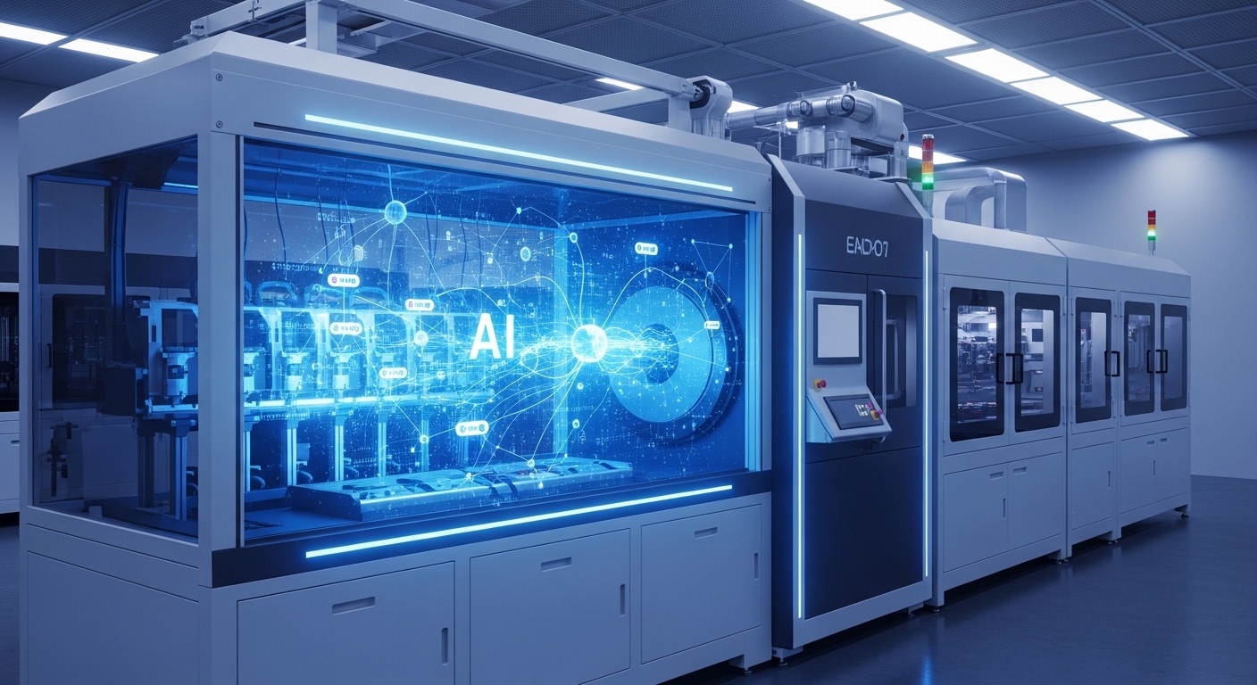
At Moore Solution Technology, we have been building AI software for semiconductor equipment since before the current wave of enterprise AI enthusiasm. Our NeuroBox platform embodies the playbook this article describes: copilot-first deployment that respects engineer expertise, process-specific models tuned to individual equipment types, deep integration with SEMI standards (GEM/SECS-II) for real-time data collection, and edge deployment architecture that works in real fab environments — not just cloud demonstrations.
Our product line spans the AI lifecycle for semiconductor equipment:
- NeuroBox D — AI-powered design automation, from P&ID to 3D equipment assembly
- NeuroBox E5200 — Smart commissioning and DOE optimization, reducing test wafer consumption by up to 80%
- NeuroBox E3200 — Production-line AI including virtual metrology, run-to-run control, and fault detection in real-time
We are not the only company that sees this opportunity. But we believe we are among the few that combine the three ingredients the a16z framework identifies as essential for vertical AI success: deep domain expertise in semiconductor manufacturing processes, production-grade AI engineering capable of operating under real-world constraints, and a go-to-market strategy that starts with high-value, low-risk entry points and expands from there.
The a16z report confirms what we have believed from the beginning: the “hard” industries are where the most durable AI companies will be built. Legal AI has Harvey. Healthcare AI has its emerging leaders. Semiconductor equipment AI does not yet have its breakout company.
That is the opportunity we are building toward.
This analysis reflects the views of the MST founding team and is based on publicly available data from a16z’s enterprise AI reports. For more on our approach to semiconductor equipment AI, visit mst-sg.com or connect with us on LinkedIn.
NeuroBox covers the full lifecycle: design automation, Smart DOE commissioning, and real-time production AI.
Explore Solutions →Review a semiconductor AI workflow with MST
From Smart DOE to VM/R2R review, project impact depends on equipment data, validation scope and customer acceptance criteria.
Book a Demo →