- →What Are the Fundamental Differences Between Edge AI and Cloud AI in Manufacturing?
- →Why Does Latency Matter So Much in Semiconductor Manufacturing?
- →How Do Data Security Requirements Favor Edge Deployment?
- →What Happens When the Network Goes Down?
- →How Does the NVIDIA Jetson Ecosystem Enable Industrial Edge AI?
Key Takeaway
Semiconductor fabs are increasingly deploying edge AI systems that deliver sub-50ms inference latency — compared to 500ms or more for cloud-based alternatives — while keeping proprietary process data on-premises. The shift is driven by three non-negotiable manufacturing requirements: real-time control loops that cannot tolerate network round-trips, data security regulations that prohibit sending wafer-level data to external servers, and operational continuity that demands AI inference even during network outages. Edge AI deployment in semiconductor manufacturing is projected to grow at 41% CAGR through 2029, with NVIDIA Jetson and industrial GPU platforms forming the compute backbone.
What Are the Fundamental Differences Between Edge AI and Cloud AI in Manufacturing?
The distinction between edge AI and cloud AI is not merely architectural — it represents a fundamentally different philosophy about where intelligence should reside in a manufacturing operation.
Cloud AI centralizes compute in remote data centers. Sensor data from the production line is collected, transmitted over the network to a cloud server, processed by AI models, and the results are sent back. This architecture excels when latency is not critical, when data volumes are manageable for transmission, and when the cost of cloud compute is lower than maintaining local infrastructure. It is the dominant model for business analytics, demand forecasting, and supply chain optimization.
Edge AI places compute directly at or near the point of data generation — on the factory floor, inside the equipment, or in a local server rack within the fab. Sensor data is processed locally, inference happens in milliseconds, and only aggregated results or anomaly alerts are sent to central systems. This architecture is essential when real-time response is mandatory, when data cannot leave the premises, or when network reliability cannot be guaranteed.
In semiconductor manufacturing, the choice between these architectures is not theoretical. A single modern fab generates 5–10 terabytes of data per day from thousands of sensors across hundreds of process tools. The physics of network transmission means that sending this data to the cloud and waiting for a response introduces latency that ranges from 200ms at best to over 2,000ms under load — latencies that are incompatible with real-time process control.
Why Does Latency Matter So Much in Semiconductor Manufacturing?
To understand why sub-50ms latency is not a luxury but a requirement, consider the control loops that govern semiconductor process quality.
In a chemical vapor deposition (CVD) chamber, gas flow rates, temperature, and pressure must be adjusted in real time based on sensor readings to maintain film thickness uniformity within nanometer tolerances. A Run-to-Run (R2R) control system that adjusts recipe parameters between wafer lots needs to compute its adjustments before the next wafer enters the chamber — a window measured in seconds, not minutes.
Virtual Metrology (VM) systems predict wafer quality from in-situ sensor data, allowing fabs to reduce physical measurement sampling from 100% to as low as 10–20%. But VM predictions are only useful if they arrive before the wafer moves to the next process step. At a typical throughput of 30–60 wafers per hour, this means the VM model must return a prediction within 30–60 seconds of data collection — and the tighter this window, the more wafers can be intercepted before defects propagate.
Edge AI systems like MST’s NeuroBox E3200 series achieve inference latency of 15–45ms for VM predictions and R2R recipe adjustments. Cloud-based alternatives, even with optimized pipelines, typically deliver 500–1,500ms latency due to network transmission, queuing, and round-trip overhead. In a process environment where every millisecond of delay increases the probability of an out-of-spec wafer, this 10–30x latency difference is decisive.
How Do Data Security Requirements Favor Edge Deployment?
Semiconductor manufacturing data is among the most sensitive industrial information in the world. Process recipes, equipment parameters, yield data, and defect patterns represent billions of dollars in accumulated R&D investment. For leading-edge foundries, this data is literally the source of competitive advantage — the reason one fab achieves 95% yield while a competitor with identical equipment achieves only 80%.
The regulatory landscape reinforces this sensitivity. China’s Data Security Law and Personal Information Protection Law impose strict controls on cross-border data transfer, particularly for data classified as “important” — a category that explicitly includes industrial process data. The EU’s GDPR and the proposed Data Act create similar constraints for European fabs. Even in the United States, the CHIPS Act’s guardrails include provisions around data handling for subsidized fab operations.
Cloud AI architectures, by definition, require data to leave the production environment. Even when cloud providers offer dedicated instances and encrypted transmission, the data physically traverses networks and resides on infrastructure controlled by a third party. For many fab operators, this is a non-starter — not because the cloud provider is untrustworthy, but because the compliance burden and risk surface of cloud-based processing exceed the operational benefits.
Edge AI eliminates this concern entirely. All data stays within the fab’s physical and network perimeter. The AI models run on hardware that the fab controls. Audit trails are local. And compliance teams can verify data handling without negotiating with external cloud providers.
What Happens When the Network Goes Down?
Network reliability is the often-overlooked factor that makes edge AI essential for manufacturing. A semiconductor fab operates 24/7/365, with planned downtime measured in hours per year. The cost of unplanned downtime ranges from $100,000 to $500,000 per hour for a modern 300mm fab, depending on the process step and wafer value.
Cloud AI systems fail when the network fails. A network outage — whether caused by ISP issues, router failures, or cyber attacks — renders cloud-dependent AI systems completely non-functional. The process tools continue to run, but without AI-driven quality predictions, recipe adjustments, or anomaly detection. Engineers must revert to manual monitoring or conservative fixed recipes, both of which degrade yield and throughput.
Edge AI systems, by contrast, operate independently of external connectivity. The NeuroBox E3200, for example, continues full inference operations during network outages, caching results locally and synchronizing with central systems when connectivity is restored. In a 2025 survey of semiconductor fab managers by SEMI, 73% cited “operation during network disruption” as a top-three requirement for any AI system deployed on their production lines.
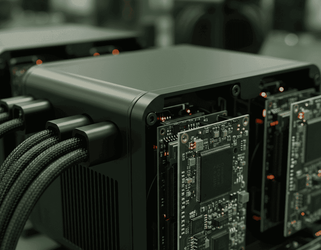
How Does the NVIDIA Jetson Ecosystem Enable Industrial Edge AI?
The hardware foundation for edge AI in manufacturing has matured dramatically in the past three years, driven largely by NVIDIA’s Jetson platform and its industrial derivatives. The Jetson Orin NX, delivering up to 100 TOPS (Trillion Operations Per Second) of AI inference performance in a module smaller than a credit card, has become the reference platform for industrial edge AI deployments.
MST’s NeuroBox architecture leverages the Jetson ecosystem along with industrial-grade GPU platforms to deliver a purpose-built edge AI appliance for semiconductor manufacturing. The hardware is designed for fab environments: fanless thermal management for cleanroom compatibility, wide temperature tolerance, industrial I/O for connecting to equipment sensors and SECS/GEM interfaces, and ESD protection rated for semiconductor production environments.
The software stack is equally important. NeuroBox runs optimized TensorRT inference engines on its edge hardware, with models trained on historical process data and continuously fine-tuned through federated learning — where model updates are shared across installations without transferring raw data. This approach combines the personalization benefits of local training with the collective intelligence benefits of fleet-wide learning.
From a cost perspective, edge deployment is increasingly competitive. A NeuroBox E3200 unit capable of serving 10–15 process tools costs a fraction of the annual cloud compute charges required to achieve equivalent throughput and latency for the same workload. When factoring in the elimination of data egress fees, reduced network infrastructure requirements, and lower compliance overhead, the total cost of ownership for edge AI is typically 35–50% lower than cloud alternatives over a three-year period.
What Does the Future Hold for Edge AI in Semiconductor Manufacturing?
The trend toward edge AI in semiconductor manufacturing is accelerating, not stabilizing. Three developments will shape the next phase.
First, the convergence of edge and cloud into hybrid architectures. Rather than choosing one or the other, leading fabs are deploying edge AI for real-time control and cloud AI for historical analytics, model training, and cross-fab benchmarking. The edge handles the millisecond decisions; the cloud handles the strategic insights. MST’s NeuroBox platform is designed for exactly this hybrid model, with seamless synchronization between edge inference and cloud-based model management.
Second, the expansion of edge AI beyond quality control into predictive maintenance, energy optimization, and autonomous process development. Each of these applications has its own latency and data security requirements, but all benefit from the same edge computing infrastructure. The NeuroBox E5200 series, focused on equipment commissioning and Smart DOE, represents this expansion — using edge AI not just to monitor production but to accelerate the process development phase that precedes it.
Third, the emergence of industry standards for edge AI interoperability. SEMI’s E187 standard for equipment data acquisition and the ongoing work on AI model exchange formats will reduce the integration burden for fab operators, making it easier to deploy and manage edge AI systems from multiple vendors within a single production environment.
For semiconductor manufacturers evaluating their AI strategy, the evidence is clear: edge AI is not an alternative to cloud AI but a necessary complement — and for real-time production applications, it is the only architecture that meets the industry’s non-negotiable requirements for speed, security, and reliability.
Discover how MST deploys AI across semiconductor design, manufacturing, and beyond.