- →What Does Equipment Commissioning Really Cost?
- →Why Is Traditional Commissioning So Inefficient?
- →How Does AI-Powered Smart DOE Transform Commissioning?
- →What Financial Impact Can Fabs Expect from AI-Powered Commissioning?
- →What Does AI-Powered Commissioning Look Like in Practice?
Key Takeaway
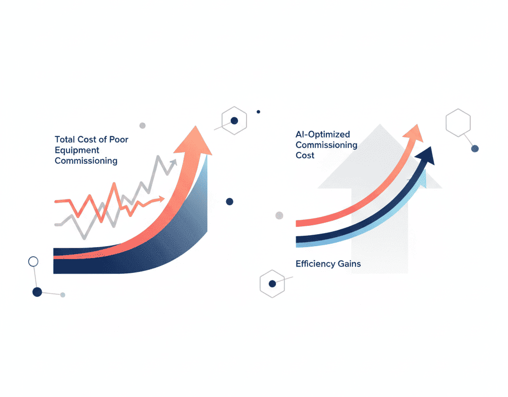
Equipment commissioning consumes 200-500 test wafers per tool at $2,000-8,000 each, costing $400K-4M per installation and taking 4-8 weeks of engineering time. AI-powered Smart DOE reduces test wafer consumption by 80% and compresses commissioning timelines by 60%, saving semiconductor fabs $15-40M annually across typical equipment installation programs.
What Does Equipment Commissioning Really Cost?
When semiconductor fabs evaluate the cost of new equipment, they focus on the capital expenditure — the $5-50M price tag for an advanced etch tool, CVD system, or lithography scanner. But the true cost of bringing that equipment into production extends far beyond the purchase price. Equipment commissioning — the process of qualifying the tool to run production recipes at acceptable quality levels — represents a substantial hidden cost that is systematically underestimated and poorly tracked.
The commissioning process involves running test wafers through progressively complex recipe sequences, measuring results, adjusting parameters, and iterating until all process specifications are met. For a complex process tool with 10-15 recipes, this typically requires 200-500 test wafers. At advanced nodes where test wafer costs range from $2,000-8,000 each (depending on the incoming process state required), the test wafer cost alone reaches $400K-4M per tool installation.
But test wafers are only one component of the total commissioning cost. Engineering labor is equally significant. A typical commissioning requires 2-3 senior process engineers working full-time for 4-8 weeks. At fully-loaded engineering costs of $150-250K annually, the labor component adds $50-150K per tool. Additional costs include qualification metrology time ($20-50K), clean room consumables, and the opportunity cost of the tool sitting idle during commissioning instead of generating revenue.
For a major fab expansion or technology migration involving 50-100 new tool installations, total commissioning costs can reach $50-200M — a figure that rarely appears in capital planning budgets but directly impacts the fab’s financial performance and time to revenue.
Why Is Traditional Commissioning So Inefficient?
Traditional equipment commissioning follows a methodology that has remained largely unchanged for three decades: experienced engineers design experiments based on their knowledge and intuition, run those experiments, analyze results, and iterate. This approach has four fundamental inefficiencies.
Redundant experimentation. Engineers typically run full factorial or large fractional factorial DOE matrices to characterize equipment behavior. For a recipe with 8 adjustable parameters, a three-level factorial design requires 6,561 runs. Even aggressive fractional designs require 81-243 runs. Many of these runs provide redundant information — they confirm what earlier runs already suggested — but traditional DOE methodology requires completing the full experimental matrix regardless.
Sequential learning. Traditional commissioning follows a sequential process: run a batch of experiments, wait for metrology results (often 4-24 hours), analyze, design the next batch, repeat. This serial workflow means that 60-70% of commissioning calendar time is spent waiting for data rather than generating it. A process that requires 200 test wafers does not take long because of the 200 wafer runs — it takes long because of the 15-20 analysis-and-redesign cycles between runs.
Knowledge loss. When an engineer commissions a tool, they develop deep intuition about that specific equipment’s behavior — which parameters interact, where the sweet spots are, how this tool differs from others of the same type. This knowledge typically resides in the engineer’s head and informal notes. When the next tool of the same type is installed, the commissioning process starts largely from scratch because the learning is not systematically captured and transferred.
Conservative margins. Because commissioning is expensive and time-pressured, engineers tend to accept “good enough” process conditions rather than optimizing to the true equipment potential. They find a recipe that meets specifications and move on, leaving potential yield and throughput improvements on the table. Studies suggest that conventionally commissioned tools typically operate 5-15% below their theoretical performance ceiling.
How Does AI-Powered Smart DOE Transform Commissioning?
AI-powered Smart DOE addresses each of these inefficiencies through a fundamentally different approach to experimental design and process optimization.
Bayesian optimization replaces factorial design. Instead of pre-defining a full experimental matrix, Smart DOE uses Bayesian optimization to select each experiment adaptively. After every test wafer, the AI model updates its understanding of the process landscape and selects the next experiment to maximize information gain. This means every test wafer teaches the system something new — there are no redundant experiments.
The practical impact is dramatic. Where traditional DOE might require 200-300 test wafers to characterize a complex recipe, Smart DOE achieves equivalent or better characterization in 40-60 wafers. That is a 70-80% reduction in test wafer consumption, translating to $320K-1.9M in savings per tool for advanced node processes.
Parallel learning accelerates timelines. Smart DOE eliminates the analysis bottleneck by providing real-time model updates as metrology data arrives. The system does not wait for the complete experimental batch to be measured before recommending next steps. As soon as data from wafer N becomes available, the model updates and can immediately recommend what wafer N+1 should run. This transforms the sequential wait-run-analyze-design cycle into a continuous flow.
MST’s NeuroBox E5200 platform further accelerates this by integrating directly with equipment automation and metrology scheduling systems. Test wafers are automatically dispatched, processed, measured, and the results fed back to the optimization model — minimizing manual touchpoints and enabling 24/7 commissioning progress even when engineers are not physically present.
Combined with the reduction in total experiments needed, Smart DOE compresses commissioning timelines from 4-8 weeks to 1-3 weeks — a 60% or greater reduction in time to production readiness.
Knowledge capture and transfer. Every Smart DOE commissioning generates a structured process model that captures the complete relationship between equipment parameters and quality outputs. This model is stored, versioned, and reusable. When the next tool of the same type is installed, the commissioning starts from the prior model rather than from zero. The system already knows the approximate parameter ranges, key interactions, and likely optimal regions — it just needs to fine-tune for the specific tool’s individual characteristics.
In practice, second-tool commissioning using transferred models requires 50-70% fewer experiments than first-tool commissioning. By the fifth tool of a type, commissioning test wafer consumption may be reduced to 15-20 wafers — a 90%+ reduction from the traditional approach.
What Financial Impact Can Fabs Expect from AI-Powered Commissioning?
The financial case for AI-powered commissioning is compelling across multiple dimensions.
Direct test wafer savings. For a fab installing 20 new tools per year (a typical expansion or technology migration rate), reducing average test wafer consumption from 300 to 60 wafers per tool saves 4,800 wafers annually. At $3,000-6,000 per test wafer, annual savings range from $14.4M to $28.8M.
Engineering productivity. Reducing commissioning time per tool from 6 weeks to 2 weeks frees 80 engineering-weeks annually across 20 tool installations. This capacity can be redirected to yield improvement, process optimization, and other high-value activities. Valued at $100-150K per engineering-year, this represents $1.5-2.9M in productivity recovery.
Faster revenue realization. Every week a tool sits in commissioning is a week it is not generating revenue. For a process tool that generates $500K-2M in monthly wafer revenue, compressing commissioning by 4 weeks accelerates revenue by $500K-2M per tool — $10-40M annually across a 20-tool installation program.
Improved process performance. Because Smart DOE optimizes more thoroughly within less time, commissioned tools start production at higher performance levels. The 5-15% performance gap between conventionally commissioned and AI-optimized tools translates to measurable yield and throughput advantages from day one of production.
Total annual financial impact for a mid-size fab: $25-70M. ROI on the AI platform investment (typically $500K-2M for commissioning capabilities): 12-35x within the first year.
What Does AI-Powered Commissioning Look Like in Practice?
To make this concrete, consider a real-world scenario: commissioning a new etch tool for advanced gate etch at the 5nm node.
Traditional approach: The process engineer reviews equipment specifications and prior commissioning records (if available). They design a fractional factorial DOE with 6 key parameters (RF power, pressure, gas ratios, temperature, bias voltage, etch time) at 3 levels each, yielding 81 experimental runs. After processing 81 test wafers over 3 days, they wait 2 days for complete metrology results. Analysis reveals the process window but indicates that two additional parameters (gas flow pulsing and chamber wall temperature) are significant. A follow-up DOE of 27 runs is designed. After another processing and measurement cycle, the engineer identifies optimal conditions, runs 15 confirmation wafers, and signs off. Total: 123 test wafers, 4 weeks, approximately $600K in test wafer costs.
AI-powered approach with MST NeuroBox E5200: The system loads the process model from the most recent commissioning of the same tool type. Starting from this prior knowledge, Bayesian optimization recommends an initial set of 8 wafers targeting the highest-uncertainty regions of the process space. Metrology results are fed back in real time. The model updates and recommends 6 more wafers, now exploring the interaction between RF power and gas pulsing that the prior model flagged as critical. After 5 such adaptive cycles and a total of 32 test wafers, the model converges on optimal conditions with high confidence. Five confirmation wafers validate the result. Total: 37 test wafers, 10 days, approximately $185K in test wafer costs.
The AI approach delivered equivalent process performance (actually 3% better etch uniformity) in one-quarter the time at one-third the cost. Multiply this across dozens of tool installations, and the strategic impact becomes clear.
Why Is Now the Right Time to Transform Your Commissioning Process?
Several industry dynamics make AI-powered commissioning increasingly urgent. Fab construction is booming — SEMI forecasts 82 new fab projects starting between 2024 and 2027, representing over $500 billion in capital investment. Each of these fabs will commission hundreds of tools, creating unprecedented demand for commissioning efficiency.
Simultaneously, the engineering talent shortage is intensifying. Experienced process engineers capable of leading equipment commissioning are in critically short supply. AI-powered commissioning does not replace these engineers — it amplifies their productivity by 3-5x, allowing a smaller team to commission more tools in less time.
The technology is mature and production-proven. MST’s NeuroBox E5200 platform has been deployed across multiple semiconductor fabs in Asia, demonstrating consistent 70-80% reductions in test wafer consumption and 50-60% reductions in commissioning timelines across various equipment types including etch, CVD, PVD, and diffusion tools.
For semiconductor executives evaluating AI investments, equipment commissioning optimization offers a uniquely attractive combination: clear ROI, fast payback, limited organizational disruption, and a natural entry point for broader AI adoption across manufacturing operations. It is, in many ways, the ideal “first AI project” for fabs beginning their digital transformation journey — and a high-impact expansion area for those already on the path.
Reduce trial wafer consumption by 80% with AI-powered Smart DOE.