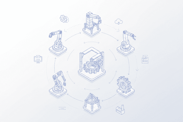
- →Why Does Equipment Design Take Longer Than Building the Actual Machine?
- →Where Exactly Does Design Time Accumulate?
- →What Makes This Problem So Difficult to Solve With Traditional Methods?
- →How Does This Bottleneck Impact Business Outcomes?
- →Can AI Actually Address the Core Design Bottleneck?
Key Takeaway
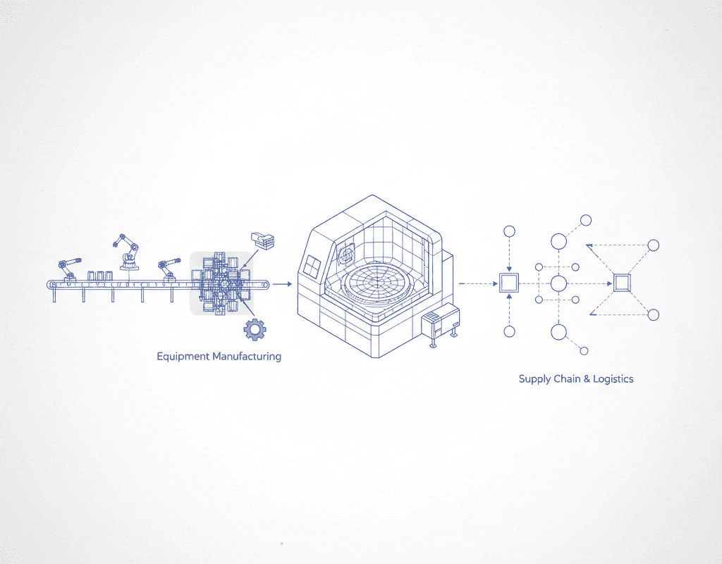
In semiconductor equipment manufacturing, design — not fabrication — is the primary schedule bottleneck. Industry data shows that mechanical and systems design consumes 35–50% of total project lead time, while physical assembly accounts for only 15–20%. Addressing design throughput with AI-driven automation can compress overall delivery timelines by 40–60%.
Why Does Equipment Design Take Longer Than Building the Actual Machine?
Ask any program manager at a semiconductor equipment OEM what keeps them up at night, and the answer is rarely the shop floor. It is the design phase. According to a 2024 survey by SEMI of 127 equipment manufacturers across Asia and North America, the median time from customer specification lock to first article shipment is 22 weeks. Of those 22 weeks, 9.4 weeks — roughly 43% — are consumed by mechanical design, systems integration design, and engineering documentation.
Physical assembly, by contrast, takes an average of 3.8 weeks. Procurement adds another 4.2 weeks. Testing and qualification account for 3.1 weeks. The math is unambiguous: design is the single largest time block in the entire delivery cycle.
This bottleneck is not caused by lazy engineers. It is structural. Semiconductor equipment — gas delivery panels, chemical mechanical planarization modules, wafer handling subsystems — involves deeply interconnected mechanical, fluid, electrical, and thermal domains. A single gas panel for an etch tool may contain 180–240 discrete components: valves, mass flow controllers, pressure regulators, filters, check valves, fittings, and tubing runs. Each must be placed, routed, and validated against process specifications, safety codes (SEMI S2, CE, NFPA 318), and manufacturing constraints.
Where Exactly Does Design Time Accumulate?
Breaking down the 9.4-week design phase reveals specific sub-tasks where time concentrates:
P&ID development and review: 1.2–2.0 weeks. Process engineers create piping and instrumentation diagrams that define every flow path, instrument tap, and safety interlock. These are the source of truth for all downstream mechanical work. Multiple review cycles with the customer can stretch this phase significantly — one major Korean OEM reported averaging 3.2 review iterations per P&ID package.
3D mechanical layout: 2.5–4.0 weeks. This is the core bottleneck within the bottleneck. Senior designers translate 2D P&ID intent into 3D SolidWorks or CATIA assemblies. They select components from vendor catalogs, position them in the chassis envelope, and route tubing or piping between connection points. A typical gas box assembly with 200 components requires 320–480 person-hours of SolidWorks time.
Design review and error correction: 1.5–2.5 weeks. Internal review catches interference issues, code violations, and manufacturability problems. Industry data from a 2023 study by the Aberdeen Group found that the average equipment design project undergoes 2.7 formal review cycles, with each cycle requiring 1.8 days of senior engineer time.
Drawing package generation: 0.8–1.2 weeks. Production drawings, BOMs, wiring diagrams, and assembly instructions must be extracted and formatted for the shop floor. This is tedious, error-prone, and universally disliked by engineers.
What Makes This Problem So Difficult to Solve With Traditional Methods?
Equipment companies have tried several approaches to accelerate design, with limited success:
Hiring more designers. The global shortage of experienced SolidWorks designers who understand semiconductor process equipment is acute. In Taiwan and South Korea, senior mechanical designers with gas system experience command salaries 40–60% above general mechanical engineering roles. Even with competitive compensation, the talent pool is finite. One Hsinchu-based OEM reported that it took 8 months to fill a single senior gas panel designer position in 2024.
Template-based design reuse. Most OEMs maintain libraries of past designs. But semiconductor equipment is highly customized — each customer fab has specific process recipes, footprint constraints, and facility interface requirements. Engineers report that template reuse covers only 30–45% of a new design, with the remaining work requiring original engineering.
PDM/PLM workflow optimization. Product data management systems improve traceability and version control, but they do not reduce the core cognitive work of 3D layout and routing. They manage the process around design rather than accelerating design itself.
How Does This Bottleneck Impact Business Outcomes?
The financial consequences are substantial. For a mid-sized equipment OEM generating $80–150M in annual revenue, design throughput directly constrains order capacity. Consider the arithmetic: if the company has 12 senior mechanical designers and each design project requires 400 person-hours of their time, the company can execute roughly 50–55 design projects per year (accounting for overhead, reviews, and non-project time).
If each project represents an average equipment value of $1.8M, design throughput caps revenue at approximately $90–99M. To grow beyond that ceiling, the company must either hire more senior designers (scarce) or find ways to compress design hours per project.
Schedule delays carry direct financial penalties. In the semiconductor equipment industry, late delivery penalties typically range from 0.5–1.5% of contract value per week of delay, capped at 10–15%. For a $2.5M tool delivery, a 4-week delay can cost $50K–150K in penalties alone, not counting the reputational damage and reduced probability of repeat orders.
Can AI Actually Address the Core Design Bottleneck?
Recent advances in AI-driven design automation are beginning to demonstrate meaningful impact on the 3D layout and routing phases — the heart of the bottleneck. Platforms like NeuroBox D by MST approach the problem by automating the translation from P&ID to 3D assembly: AI reads the process diagram, identifies components, applies engineering rules and spatial constraints, and generates a SolidWorks-compatible 3D assembly with tubing routes.
Early deployment data from three equipment manufacturers using AI-assisted design shows promising results. A gas system manufacturer in Shenzhen reported reducing gas box 3D layout time from 320 person-hours to approximately 45 person-hours — an 86% reduction. The AI-generated layout required human review and refinement, but the starting point was substantially complete rather than a blank screen.
The technology works by combining computer vision (to parse P&ID symbols and connectivity), constraint-based generative design (to position components within physical envelopes), and learned routing algorithms (to create tubing paths that satisfy minimum bend radius, accessibility, and code requirements). Tools like DrawingDiff add a layer of automated design review, comparing revisions and flagging discrepancies that human reviewers might miss.
The critical insight is that AI does not need to replace the designer. It needs to eliminate the 60–70% of design time spent on mechanical placement and routing — tasks that are rule-governed but labor-intensive. The designer expertise is then focused on the 30–40% of work that genuinely requires engineering judgment: novel configurations, edge cases, and optimization.
What Should Equipment Companies Do About This Bottleneck Today?
For equipment OEMs evaluating their design operations, several steps are actionable now:
Measure your actual design-to-build ratio. Track person-hours from specification receipt to design release versus design release to shipment. If design exceeds 40% of total lead time, you have a structural bottleneck worth addressing.
Audit your component library completeness. AI-driven design automation is only as effective as the parts database it draws from. Companies with well-organized, parametric component libraries (including 3D models, connection specifications, and procurement data) will see faster ROI from automation tools.
Identify your highest-volume, most-repeatable design categories. Gas panels, chemical delivery systems, and wafer handling subsystems tend to be the best candidates for AI-assisted design because they have well-defined component vocabularies and design rules.
Pilot AI design tools on a specific product line. Rather than attempting a company-wide transformation, select one product family where you have strong historical data and clear design standards. Measure cycle time reduction against your baseline.
The semiconductor equipment industry is entering a period of unprecedented demand driven by AI chip manufacturing, advanced packaging, and geographic diversification of fab capacity. Companies that can deliver equipment faster without sacrificing design quality will capture disproportionate market share. The hidden bottleneck in design is no longer hidden — and the tools to address it are becoming available.
Still designing assemblies manually?
NeuroBox D converts your P&ID into a complete SolidWorks assembly — in hours, not days. See how it works with your own designs.
NeuroBox D generates native SolidWorks 3D assemblies from P&ID in 4 hours. Auto BOM, zero errors.
Book a Demo →See how NeuroBox reduces trial wafers by 80%
From Smart DOE to real-time VM/R2R — our AI runs on your equipment, not in the cloud.
Book a Demo →