- →Why Is the Semiconductor AI Market So Fragmented?
- →What Problems Does Fragmentation Create for Fab Operations?
- →What Does the Consolidation Pattern Look Like?
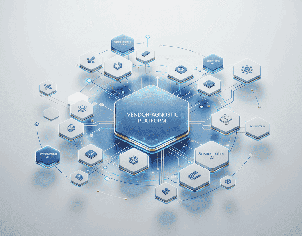
- →Why Do Vendor-Agnostic Platforms Have a Structural Advantage?
- →How Should Fab Leaders Evaluate AI Platform Decisions?
Key Takeaway
The semiconductor AI market is fragmenting into 200+ point solutions — creating integration nightmares for fabs running 30-50 different tools from 10+ OEMs. History shows that vendor-agnostic platforms that unify data across equipment types will consolidate the market, just as ERP did for enterprise software. Fabs choosing single-vendor AI lock-in today will face 3-5x switching costs within three years.
Why Is the Semiconductor AI Market So Fragmented?
Walk the floor of SEMICON West or SEMICON Taiwan and you will encounter a bewildering landscape: over 200 companies now claim AI capabilities for semiconductor manufacturing. There are startups for predictive maintenance, separate vendors for virtual metrology, another set for recipe optimization, yet another for yield analytics, and dozens more for specific niches like defect classification or chamber matching.
This fragmentation is not accidental — it mirrors the early stages of every enterprise software market. In the 1990s, manufacturers used separate systems for accounting, inventory, scheduling, and procurement. It took a decade of painful integration before ERP platforms like SAP consolidated these functions. The semiconductor AI market is at the same inflection point.
The numbers tell the story: the global semiconductor AI market is projected to reach $4.1 billion by 2028 (MarketsandMarkets, 2024), growing at 24.3% CAGR. But the average large fab now manages 12-15 different AI or analytics tools from 8-10 different vendors. Each tool has its own data format, its own deployment model, its own support contract, and its own training requirement. The total cost of ownership for this fragmented approach is 3-5x higher than an integrated platform.
What Problems Does Fragmentation Create for Fab Operations?
The practical impact of AI fragmentation hits fabs in four critical areas:
Data silos destroy cross-tool intelligence. A predictive maintenance system monitoring an etch tool cannot communicate with the virtual metrology system on the downstream deposition tool. When an etch chamber drifts, the downstream impact on film thickness is invisible until physical metrology catches it — often 4-8 hours and 200+ wafers later. An integrated platform that sees both tools simultaneously can catch the cascade in minutes.
Integration costs consume the AI budget. Fabs report spending 40-60% of their AI budget on integration, middleware, and custom connectors rather than on actual intelligence. A 300mm fab with $5 million in annual AI spend may be burning $2-3 million just keeping point solutions connected. That is money that generates zero analytical value.
Vendor lock-in limits equipment flexibility. When an AI solution only works with one OEM’s equipment, the fab loses negotiating leverage on tool purchases. If your Applied Materials-specific AI platform cannot handle the Lam Research tools you want to add, you are trapped. In an industry where a single tool costs $5-50 million, that constraint directly impacts capital allocation.
Talent fragmentation compounds the skills gap. Each point solution requires dedicated training. A fab running 12 AI tools needs engineers proficient in 12 different platforms. Given the existing semiconductor talent shortage of 67,000 engineers globally (SEMI, 2024), this fragmentation makes an already critical problem worse.
What Does the Consolidation Pattern Look Like?
Enterprise software markets follow a predictable consolidation curve. In the early phase (where semiconductor AI is today), hundreds of point solutions compete. In the growth phase, platform players emerge that integrate multiple capabilities. In the mature phase, 3-5 dominant platforms serve 80% of the market.
The semiconductor AI market is entering the growth phase. The signals are clear:
Major OEMs are expanding their software stacks. Applied Materials (through its AIx platform), KLA (through Litho Analyzer and other tools), and Lam Research are all building broader AI capabilities. But OEM platforms have an inherent limitation: they optimize for their own equipment. A fab running tools from 5 different OEMs cannot rely on any single OEM’s platform for holistic optimization.
Cloud hyperscalers are entering the space. AWS, Azure, and Google Cloud all have semiconductor manufacturing solutions. But cloud platforms face latency and data sovereignty challenges — real-time equipment control requires sub-100ms response times, which cloud architectures cannot guarantee.
This creates the strategic opening for vendor-agnostic, edge-deployed AI platforms. Companies that can ingest data from any equipment maker via standard protocols (SECS/GEM, EDA/Interface A, OPC-UA), run inference at the edge with sub-millisecond latency, and provide a unified analytics layer across all tools are positioned to become the de facto integration standard.
Why Do Vendor-Agnostic Platforms Have a Structural Advantage?
The economics strongly favor platform approaches over point solutions for three reasons:
Cross-tool learning creates a data moat. Every tool a vendor-agnostic platform connects to increases the value of its models. A platform monitoring 10,000 tools across 50 fabs has vastly more training data than a point solution deployed on 500 tools. Transfer learning across tool types (e.g., applying etch chamber insights to CVD chamber models) multiplies this advantage. Platform economics follow Metcalfe’s Law: value grows proportionally to the square of connected nodes.
Deployment costs decrease with scale. A platform with standardized connectors for SECS/GEM, EDA, and common data historians can onboard a new tool type in days rather than months. Point solutions that require custom integration for each deployment cannot match this efficiency. For a fab adding 50 new tools per year, the deployment cost difference alone can reach $500,000 annually.
Upgrade paths are unified. When a platform releases a new algorithm — say, a better anomaly detection model — every connected tool benefits simultaneously. Point solutions require tool-by-tool upgrades, each with its own testing and validation cycle. In a regulated environment where change control can take weeks, this difference compounds rapidly.
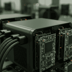
MST’s NeuroBox architecture exemplifies this approach. The E3200 production platform connects to any SECS/GEM-compliant tool, runs VM, R2R, FDC, and EIP algorithms from a single edge node, and shares learned models across tool types. A drift pattern identified on one CVD chamber can be immediately applied as a monitoring template to every similar chamber in the fab.
How Should Fab Leaders Evaluate AI Platform Decisions?
When evaluating AI solutions, decision-makers should apply five criteria that separate platform plays from point solutions:
Protocol coverage: Does the platform support SECS/GEM, EDA/Interface A, OPC-UA, and MQTT natively? Or does it require custom connectors for each equipment type? Native multi-protocol support is the foundation of vendor-agnostic operation.
Algorithm breadth: Does the platform offer VM, R2R, FDC, SPC, predictive maintenance, and recipe optimization from a single deployment? Or do you need separate installations for each capability? Each additional deployment multiplies maintenance costs.
Edge-cloud architecture: Can the platform run real-time control loops at the edge while aggregating analytics in the cloud? Pure-cloud solutions cannot meet real-time requirements. Pure-edge solutions cannot leverage cross-fab learning. The right answer is a hybrid architecture.
Model portability: Can models trained on one tool type be transferred to similar tools? Can models move between fabs? Transfer learning and model portability are the hallmarks of platform-grade AI, and they drastically reduce time-to-value for each new deployment.
Total cost of ownership: Calculate the full cost including licensing, integration, training, maintenance, and opportunity cost of data silos. A platform at $500K per year that replaces five point solutions at $150K each is not just cheaper — it is strategically superior because it eliminates integration overhead entirely.
What Will the Semiconductor AI Landscape Look Like by 2028?
Based on historical consolidation patterns and current market dynamics, the semiconductor AI market will likely consolidate around three tiers:
Tier 1: Integrated platforms (3-5 players, 60% market share). Vendor-agnostic platforms that span the full manufacturing lifecycle — from equipment design and commissioning through production optimization and yield management. These platforms will serve as the central nervous system of the smart fab.
Tier 2: OEM-embedded solutions (5-8 players, 25% market share). Equipment makers will continue offering AI capabilities bundled with their tools. These will excel at single-tool optimization but will not provide cross-tool or cross-vendor intelligence.
Tier 3: Specialized point solutions (50+ players, 15% market share). Niche solutions for specific applications (e.g., lithography simulation, specific defect types) will survive where deep domain expertise outweighs platform integration benefits.
For fab operators making AI platform decisions today, the strategic imperative is clear: choose vendor-agnostic platforms that can grow with your operation, connect to any equipment, and provide unified intelligence across your entire manufacturing line. The switching cost of locking into the wrong platform now will only increase as your data and model dependencies deepen.
The semiconductor AI market is consolidating. The question for every fab leader is simple: will you be on the winning platform, or will you be paying 3-5x switching costs three years from now?
Discover how MST deploys AI across semiconductor design, manufacturing, and beyond.