- →The $4 Million Problem No One Talks About
- →How We Got Here: Traditional DOE Methods
- →A Different Approach: AI-Driven Smart DOE
- →How MST Implements Smart DOE
- →The Math: What Smart DOE Saves
Key Takeaway
Smart DOE reduces semiconductor equipment commissioning test wafers by 80% and cuts qualification time by 60%. Using Bayesian optimization and transfer learning, MST’s NeuroBox E5200 achieves full tool qualification in 10-15 wafers instead of 50-100, and subsequent tools need only 2-5 wafers. For a 10-tool fleet, this translates to saving 1,500+ test wafers and $300K-$2M in commissioning costs.
The $4 Million Problem No One Talks About
Your customer just bought 10 etch tools. Congratulations — that’s a $50M order. Now here’s the part the sales team doesn’t mention: before a single production wafer runs, you’re burning through 2,000 to 5,000 test wafers just to qualify those tools.
At $50-$200 per 300mm wafer, that’s $100K to $1M in silicon alone. Add in the engineering hours — typically 4 to 8 weeks per tool — and the fully loaded cost of commissioning a single tool runs $400K to $4M. Multiply by 10 tools, and you’ve got a line item that makes your CFO ask uncomfortable questions.
You’ve been there: it’s 3am, you’re on wafer #47, and the Cpk is still at 0.9. The senior PE who “just knows” the right settings retired last quarter. The recipe from Tool #1 doesn’t transfer cleanly to Tool #2. And every wasted wafer is money and time your customer didn’t budget for.
This is the commissioning problem. And it’s been solved the same way for 30 years — until now.
How We Got Here: Traditional DOE Methods
Design of Experiments isn’t new. Fisher introduced it in the 1930s for agriculture. Semiconductor adapted it in the 1980s. The core methods haven’t changed much since.
Full Factorial DOE
The textbook approach. If you have 5 parameters with 3 levels each, that’s 35 = 243 experiments. You capture every interaction, every curvature. It’s also completely impractical when each experiment costs a wafer and 45 minutes of chamber time. Nobody runs full factorial on production equipment.
Fractional Factorial DOE
The compromise. Use a 25-2 design to cut the runs from 32 to 8. But you’re aliasing interactions — and in semiconductor processing, interactions matter. That pressure × temperature interaction you aliased away? That’s exactly the one causing your uniformity excursion on the edge dies.
OFAT (One Factor at a Time)
Let’s be honest: this is what most PEs actually do. Sweep RF power from 500W to 800W, pick the best, then sweep pressure from 20mT to 60mT. It’s intuitive, it’s simple, and it misses every single interaction effect. OFAT finds a local optimum and calls it done. On a 5-parameter space, you might run 50-100 wafers and still not find the global best recipe.
Response Surface Methodology (RSM)
Better. Central Composite or Box-Behnken designs let you model curvature with fewer runs. But RSM still assumes you know which factors matter, still requires a screening phase, and still needs a human to interpret results and design the next iteration. Three rounds of RSM easily adds up to 60-80 wafers and 3 weeks of engineering time.
The Real Problem
None of these methods learn. Every tool starts from scratch. The knowledge that “this chamber type likes 15% higher RF power when the showerhead gap is at the narrow end of spec” — that lives in a senior PE’s head, not in your system. When that PE leaves, the knowledge leaves with them.
A Different Approach: AI-Driven Smart DOE
What if each wafer you ran was chosen to teach the system as much as possible? What if knowledge from one tool automatically transferred to the next? That’s the core idea behind Smart DOE.
Bayesian Optimization: Smarter Wafer Selection
Instead of pre-planning all experiments upfront, Bayesian Optimization builds a probabilistic model — typically a Gaussian Process — of the entire response surface after each run. The model tells you two things:
- Prediction: What etch rate, uniformity, or selectivity to expect at any recipe point
- Uncertainty: How confident the model is at each point
An acquisition function then picks the next experiment by balancing exploitation (running where the model predicts good results) and exploration (running where the model is uncertain). The result: every wafer is maximally informative.
In practice, this means 10-15 intelligently chosen wafers map the same response surface that OFAT needs 50-100 random walks to approximate.
Active Learning: Every Wafer Counts
Traditional DOE treats all experimental points as equally valuable. Active Learning flips this — it prioritizes experiments in regions where the model’s uncertainty is highest or where the predicted response is near the target specification boundary. You’re not just collecting data; you’re surgically eliminating uncertainty.
After 5 wafers, the model might know that pressure below 30mT always gives poor selectivity. It won’t waste wafers #6-15 confirming that. Instead, it focuses on the narrow band where pressure, power, and gas ratio interact to produce the sweet spot.
Transfer Learning: Tool #2 Is Easier Than Tool #1
This is where the compounding value kicks in. Once you’ve qualified Tool #1, the model has learned the general shape of the response surface for that process. Tool #2 — same model, same chamber design, slightly different hardware offsets — doesn’t need to learn from scratch.
Transfer Learning starts Tool #2’s model from Tool #1’s posterior. The system only needs to learn the delta — the tool-to-tool variation. In practice:
- Tool #1: 10-15 wafers (full Smart DOE)
- Tool #2: 2-5 wafers (transfer learning)
- Tool #3-10: 2-3 wafers each (model gets more confident with each tool)
For a 10-tool fleet, that’s roughly 30-50 total wafers instead of 500-1,000 with traditional methods. That’s not incremental improvement — that’s an order of magnitude.
Physics-Informed Priors: Don’t Start From Zero
A naive AI would treat etch rate vs. RF power as a completely unknown function. But we know the physics: ion energy scales with power, etch rate increases monotonically (within the power range), and there’s a threshold below which plasma doesn’t sustain.
By encoding these physics relationships as prior distributions in the Gaussian Process, the model starts with reasonable expectations. It doesn’t waste wafers “discovering” that zero RF power produces zero etch rate. This is especially important in the first 3-5 wafers, where every data point matters.
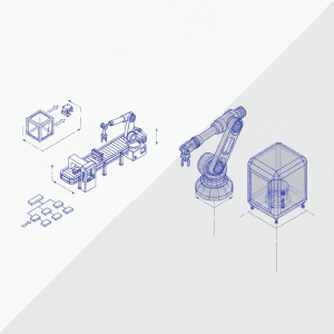
How MST Implements Smart DOE
Theory is nice. Implementation is what matters in a fab. Here’s how NeuroBox E5200 turns Smart DOE from a research concept into a production tool.
Direct Equipment Integration via SECS/GEM
NeuroBox E5200 connects directly to equipment through SECS/GEM (SEMI E5/E37) protocol — the same interface your host system uses. It reads process parameters, trace data, and equipment state in real time. No manual data entry, no CSV exports, no “let me copy these 47 parameters into Excel.”
The system ingests:
- Recipe parameters: setpoints, ramp rates, step times
- Trace data: actual vs. setpoint for every sensor, every second
- Equipment state: chamber hours, consumable life, maintenance history
- Metrology results: thickness, CD, uniformity from inline or offline measurements
This closed-loop integration means the system can recommend the next experiment, the engineer approves it, and the recipe is loaded — all within minutes, not hours.
The Smart DOE Engine
Here’s what a typical Smart DOE commissioning session looks like:
- Define targets: Enter your process specs — etch rate 200±10 nm/min, uniformity <3% 1σ, selectivity >5:1
- Set parameter ranges: RF power 400-800W, pressure 15-50mT, gas flow 100-300 sccm, etc.
- Run initial batch: The engine designs the first 3-5 experiments using a space-filling design informed by physics priors
- Iterate: After each wafer, the Bayesian model updates and recommends the next experiment
- Converge: Typically by wafer 10-15, the model has found a recipe meeting all specs with Cpk > 1.33
The entire process takes 1-3 days instead of 4-8 weeks. The engineer’s role shifts from “guess and check” to “review and approve.”
Results in the Field
Across commissioning projects, NeuroBox E5200 Smart DOE delivers:
- 80% fewer test wafers: 10-15 wafers vs. 50-100 for comparable qualification
- 60% faster commissioning time: days instead of weeks per tool
- Tool-to-tool transfer: 2-5 wafers for subsequent tools after Tool #1
- Higher final Cpk: systematic optimization finds better recipes than manual iteration
- Knowledge retention: the model captures what used to live in one PE’s head
Edge Deployment: Your Data Stays in Your Fab
NeuroBox E5200 runs at the edge — physically deployed in the fab, on-premise. Process data, recipes, and metrology results never leave your network. No cloud dependency, no data sovereignty concerns, no bandwidth bottlenecks. This isn’t negotiable for most fabs, and it shouldn’t be.
The Math: What Smart DOE Saves
Let’s run the numbers for a realistic scenario: qualifying 10 etch tools at a 300mm fab.
| Traditional DOE | Smart DOE | |
|---|---|---|
| Wafers per first tool | 80 | 12 |
| Wafers per subsequent tool | 60 | 3 |
| Total wafers (10 tools) | 620 | 39 |
| Wafer cost ($100/wafer) | $62,000 | $3,900 |
| Engineering weeks | 40-80 | 4-8 |
| Time to production | 4-6 months | 2-4 weeks |
The wafer cost savings alone are significant. But the real value is time to production. Getting 10 tools qualified 3-5 months earlier means millions in additional revenue from wafers that are now running production instead of sitting in qualification limbo.
Who Benefits Most
Smart DOE delivers the highest ROI in two scenarios:
Equipment Suppliers (OEMs)
If you build and deliver equipment, commissioning is your cost center. Every extra week on-site is an engineer who isn’t supporting the next install. Smart DOE turns your most experienced PE’s knowledge into a transferable model. New hires can run commissioning with AI guidance instead of needing 5 years of tribal knowledge.
High-Volume Fabs
If you’re qualifying multiple tools of the same type, transfer learning is your force multiplier. The marginal cost of qualifying each additional tool drops dramatically after the first one. For a fab bringing up a new line with 20-50 tools of the same type, the savings run into the millions.
Getting Started
Smart DOE isn’t a research project — it’s production-ready and deployed on NeuroBox E5200 today. If you’re spending weeks on tool qualification or burning through hundreds of test wafers per tool, there’s a faster way.
See the Impact on Your Operation
Plug in your tool count, wafer cost, and current qualification time. The calculator does the rest.
Reduce trial wafer consumption by 80% with AI-powered Smart DOE.