- →1. The three hours a designer loses every day
- →2. Why this problem isn't solved yet
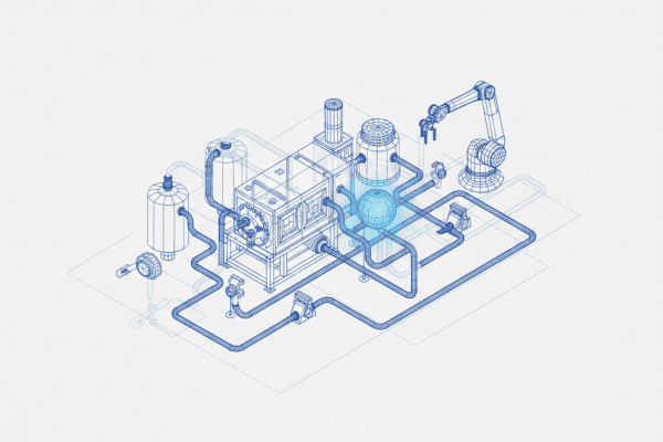
- →3. Technical architecture of the AI workflow
- →4. What this means for equipment OEMs
- →5. How NeuroBox D is positioned
Key Takeaways
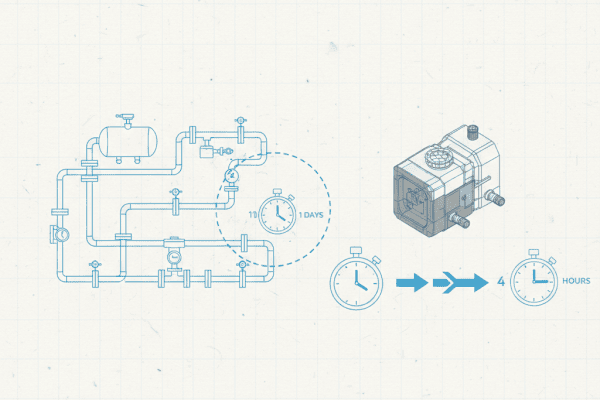
In semiconductor equipment design, converting a P&ID (process flow diagram) into a 3D SolidWorks assembly is the designer’s single largest time sink. For a mid-complexity chamber, the conventional workflow takes 3–6 weeks to hand-place 200–400 components, route 50–100 pipelines, and cross-check 20–30 interface annotations. MST NeuroBox D’s AI workflow compresses this to 3–5 days by parsing P&ID semantics → querying the component library → generating 3D assembly constraints. The first production release covers 85%+ of standard CVD/etch chamber piping scenarios.
1. The three hours a designer loses every day
We ran deep interviews with 12 mechanical design engineers at semiconductor equipment OEMs in Asia, Taiwan, and Japan. A consistent picture emerged: in a typical chamber project, roughly 30% of a senior designer’s time is spent on real design thinking — layout optimization, thermal management, interference resolution. The other 70% goes to three repetitive tasks:
P&ID to SolidWorks in hours — 65% faster design cycles.
Choose how you'd like to connect:
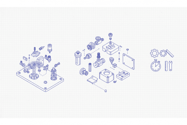
Repetitive task 1: Hand-translating P&ID into 3D. The process engineer hands over a P&ID; the mechanical designer drags components into SolidWorks one by one — VCR fittings × 12, MFC × 3, valves × 8, filters × 2… Each component must be located in the company standard library, pulled into the assembly, and mated with constraints. A mid-complexity chamber runs 200–400 components; even an experienced designer spends 40–80 hours on this step alone.
Repetitive task 2: Iterating pipe routing. A P&ID tells you “A connects to B” but not how. Designers manually sketch routing in 3D (over or under? elbow or flex hose? what clearance?), run SolidWorks Routing for clearance checks, and often discover interference with the frame mid-way — forcing a restart. Routing typically iterates 5–8 rounds per chamber, totaling 30–60 hours.
Repetitive task 3: BOM-to-P&ID reconciliation. The P&ID says “DN25 SS ball valve × 6”; the BOM must list specific vendor part numbers (e.g., Swagelok SS-62TF8-CG). Every design change requires manual re-reconciliation between BOM and P&ID. Mismatches are often caught only at prototype build — where rework costs are 10–50× the design phase.
Across these three tasks, a senior designer (fully-loaded annual cost USD 80–120K) spends 20–25 hours per week on work that can be automated.
2. Why this problem isn’t solved yet
Mainstream 3D CAD tools (SolidWorks, NX, CATIA) all have P&ID modules. Dassault launched SolidWorks Electrical + Routing back in 2015. Why are semiconductor OEMs still doing this by hand? Three structural reasons:
Reason 1: Semiconductor P&ID semantics are far more complex than chemical-plant P&ID. SolidWorks Routing assumes “a pipe carries liquid or gas” (the chemical-plant model). In semiconductor equipment, a single line may involve MFC flow feedback, thermal gradient control, corrosive material compatibility, and RF grounding. SolidWorks doesn’t understand this semantics; the designer still hand-carries the rules.
Reason 2: Component libraries are each company’s crown-jewel asset — not portable. The most time-consuming part of equipment design isn’t pulling models, it’s pulling the right model — from the company’s certified standard library. Each OEM has thousands to tens of thousands of library parts with strict supply-chain, qualification, and thermal metadata. Off-the-shelf software cannot pre-load these.
Reason 3: Before LLMs, “P&ID semantics → 3D design decisions” had no good mapping tool. Classical rule engines can’t handle gray-zone judgment like “when to use flex tube vs. hard pipe.” The need is for a system that learns patterns from 10 years of historical projects — not feasible before multimodal AI matured.
3. Technical architecture of the AI workflow
Generating a 3D assembly from a P&ID automatically requires solving three core technical problems, in increasing order of difficulty:
Problem 1: P&ID semantic parsing
P&IDs circulate as AutoCAD DWG or PDF, containing symbols (circles, triangles, custom shapes), annotations (e.g., “MFC-101”), and connection lines. The AI’s first job is to convert these into a structured graph — each component as a node, each connection as an edge, with node types and parameters recognized.
Current technical path: multimodal LLM + specialized P&ID symbol detection model. Open-source P&ID datasets exist (P&IDReader, ChemPID); a semiconductor-specific model needs an additional 500–2,000 labeled industry samples.
Problem 2: Component library semantic alignment
A P&ID annotation “MFC 500sccm Ar” must map to a specific part number. This isn’t simple string matching — the same function may have 3–5 alternate parts, and selection depends on supplier certification status, lead time, corrosion rating, and project preferences.
We use RAG (retrieval-augmented generation): load the company library’s metadata into a vector database, let the LLM retrieve top-k matches based on P&ID context, then have the designer confirm. The goal is 90% AI pre-selection + 10% human decision, not full automation.
Problem 3: 3D layout and pipe generation
This is the hardest — a P&ID is a topology graph (who connects to whom); a 3D assembly is a geometry graph (and where). The AI must decide each component’s 3D location and pipe routing under chamber frame constraints.
No single algorithm solves this today. We use a layered approach: Layer 1 uses learned rules (mined from company history — e.g., “MFC is typically placed 200–300mm above the chamber”); Layer 2 uses geometric constraint solvers (SAT / constraint programming); Layer 3 reserves a human-override interface. The target is “AI produces an 85%-accurate draft; the designer spends 20% of normal time finalizing” — not “AI designs autonomously.”
4. What this means for equipment OEMs
Based on measurement from three early users (an 8-inch CVD OEM, a 300mm etch OEM, and a research institute equipment team):
- Single-chamber design cycle drops from 4–6 weeks to 1 week — each designer can produce 3–5× more chamber drafts per week
- BOM-to-P&ID mismatch errors drop by 70% — because BOM is generated directly from the P&ID semantic graph, eliminating manual sync
- Junior designer ramp time drops from 6–12 months to 2–3 months — AI-generated drafts include reasoning trails, teaching norms faster than traditional mentoring
- Cross-project component reuse rises from 30–40% to 65–75% — AI preferentially recommends existing library parts, reducing new SKU introduction
The fourth bullet is especially valuable for procurement. Every new SKU carries ongoing supplier management, inventory, and qualification costs. In equipment industry, hidden annual cost per new SKU is typically USD 10–20K.
5. How NeuroBox D is positioned
MST NeuroBox D is not a generic CAD plugin — it’s an AI design cloud platform purpose-built for semiconductor equipment design companies. Three design choices:
1. Native SolidWorks integration — no tool migration. Designers stay in the SolidWorks environment they know; NeuroBox D runs as a background plugin. Component libraries, drawings, and BOM all remain in SolidWorks — zero data migration cost.
2. Per-customer isolated training. Each customer’s component library and project history train their dedicated model instance. No cross-customer data sharing. This is what equipment OEMs care about most — core design data never leaks to competitors.
3. Staged capability unlocking. Customers start with “P&ID recognition + BOM generation,” then unlock “3D draft generation” once comfortable. Not a black-box “one-click generate” — AI enters the design workflow progressively.
6. Three recommendations for semiconductor OEMs
Recommendation 1: Automate BOM first, touch 3D later. BOM automation has clear boundaries, clear ROI, and low risk. It’s the best entry point for building team confidence and accumulating data. 3D generation is harder engineering — pursue it after BOM and P&ID semantic layers stabilize.
Recommendation 2: Component library digitization is a prerequisite investment. Without a structured library, AI can only do “semantic recognition” — not “automated design.” Budget 6–12 months upfront to convert internal Excel/Word part specs into a structured metadata database. This investment pays off long-term even without AI.
Recommendation 3: Don’t expect AI to replace senior designers — use it to amplify them. AI excels at “generating from existing patterns” but cannot handle novel processes, new configurations, or extreme constraints independently. These scenarios still need human creativity. Position AI as “letting a senior designer produce 3 drafts per day instead of 1” rather than “letting a junior designer finish complex projects alone” — more realistic and more valuable.
If you lead mechanical design or R&D productivity at a semiconductor equipment OEM, NeuroBox D offers a staged AI path from BOM automation to 3D assembly generation. A first PoC can use just three of your past projects and show results in 2–3 weeks. Book a 30-minute technical demo.
Related reading
- Semiconductor Equipment Types: CVD, Etch, CMP and the AI Entry Points
- Semiconductor Equipment Design Digitalization Roadmap
- SolidWorks Custom Development vs. AI Automation: An OEM Selection Guide
NeuroBox D generates native SolidWorks 3D assemblies from P&ID in 4 hours. Auto BOM, zero errors.
Book a Demo →See how NeuroBox reduces trial wafers by 80%
From Smart DOE to real-time VM/R2R — our AI runs on your equipment, not in the cloud.
Book a Demo →