Key Takeaway
AI is transforming every stage of semiconductor manufacturing in 2026. Key trends: AI-powered design automation reducing equipment design time by 60%, Smart DOE cutting trial wafers by 80%, Virtual Metrology enabling 100% quality coverage, and predictive maintenance improving equipment uptime by 15-25%.
The semiconductor industry is undergoing a fundamental transformation driven by artificial intelligence. From design automation to yield optimization, AI is reshaping every stage of the chip manufacturing process.
Key trends driving this transformation include:
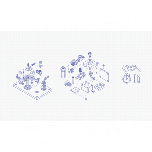
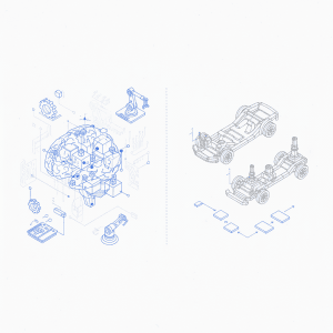
- AI-Powered Design: Automated conversion of P&ID diagrams to 3D assembly models is reducing design cycles from weeks to hours.
- Smart Equipment Commissioning: Machine learning algorithms are dramatically reducing the number of test wafers needed during equipment setup, cutting costs and time-to-production.
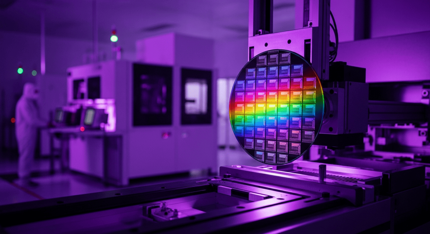
- Real-Time Process Control: Advanced AI models enable virtual metrology and run-to-run control, maintaining tighter process windows and improving yield.
- Energy Management: AI-driven energy optimization platforms are helping fabs reduce power consumption while maintaining output quality.
As the industry moves toward more complex process nodes, the role of AI in semiconductor manufacturing will only grow more critical. Companies that embrace AI infrastructure today will have a decisive competitive advantage in the years ahead.
Discover how MST deploys AI across semiconductor design, manufacturing, and beyond.