- →What Is Chamber Matching and Why Does It Matter?
- →How Does the Traditional Golden Wafer Method Work?
- →How Does AI-Driven Chamber Matching Work Differently?
- →What Results Does AI Chamber Matching Deliver?
- →How Does AI Handle Multi-Tool, Multi-Chamber Complexity?
Key Takeaway
Traditional golden wafer chamber matching is expensive, infrequent, and provides only point-in-time snapshots. AI-driven chamber matching uses continuous sensor data analysis to maintain tool-to-tool consistency in real time, reducing matching-related yield loss by 25-40% while eliminating the need for dedicated matching wafers that cost $500-2,000 each.
In a modern 300mm semiconductor fab, a single process step — say, plasma-enhanced CVD for silicon nitride deposition — might run across four identical chambers on the same tool, and across three identical tools on the production floor. That is twelve chambers, each expected to produce film thickness within a 1-2% tolerance of the target, with uniformity better than 1% across the 300mm wafer surface.
In theory, these chambers are identical. They were manufactured to the same specification, installed in the same cleanroom, and configured with the same process recipe. In practice, no two chambers are ever truly the same. Manufacturing tolerances in hardware components, subtle differences in gas delivery plumbing, variations in RF power coupling, and accumulated process history create chamber-to-chamber differences that drift over time.
Managing these differences — chamber matching — is one of the most time-consuming, costly, and frustrating tasks in semiconductor manufacturing engineering.
What Is Chamber Matching and Why Does It Matter?
Chamber matching is the process of ensuring that wafers processed in any chamber on any tool produce statistically equivalent results. When matching is good, wafers can be routed to any available chamber without affecting yield. When matching degrades, wafers processed in a drifting chamber produce out-of-specification results — thinner films, higher defect counts, shifted electrical parameters — that may not be detected until downstream metrology or, worse, final test.
The financial impact is substantial. A 2024 analysis published in IEEE Transactions on Semiconductor Manufacturing estimated that chamber mismatch accounts for 8-15% of total yield loss in advanced logic fabs. For a fab producing $5 billion in annual revenue, that represents $400-750 million in preventable losses.
The impact extends beyond yield. Poor chamber matching reduces scheduling flexibility — if two of twelve chambers are out of specification, the remaining ten must absorb the full production load, creating bottlenecks. It increases engineering overhead — process engineers spend an estimated 15-20% of their time on matching-related activities. And it complicates root cause analysis — when a yield excursion occurs, the first question is always “which chamber?” rather than “which process parameter?”
How Does the Traditional Golden Wafer Method Work?
The industry-standard approach to chamber matching uses “golden wafers” — specially prepared test wafers that are processed through each chamber under controlled conditions and then measured to compare results across chambers.
The typical golden wafer matching procedure works as follows: A set of 25 bare silicon or test-pattern wafers is prepared with precise incoming specifications. Each wafer is processed through a single chamber using the production recipe. After processing, each wafer is measured on a metrology tool — ellipsometry for film thickness, four-point probe for sheet resistance, KLA-Tencor inspection for defects. The measurement results are compiled into a matching report that compares chamber-to-chamber variation against specification limits.
When chambers are within specification, the report is filed and production continues. When chambers exceed matching limits, process engineers adjust recipe parameters — RF power, gas flows, temperature setpoints, pressure — to bring the drifting chamber back into alignment. The adjustment is followed by another golden wafer run to verify the correction. This iterate-adjust-verify cycle can consume 3-5 days and 50-100 test wafers per matching event.
The problems with this approach are fundamental:
Point-in-time measurement. Golden wafer matching provides a snapshot of chamber condition at the moment of the test. Between matching events — which are typically performed monthly or quarterly — chambers can drift without detection. A chamber that was well-matched on Monday can be out of specification by Wednesday due to a gradual shift in gas delivery or RF coupling.
Production disruption. Running golden wafers requires taking chambers offline for the test, reducing available production capacity. For high-volume fabs where every chamber-hour has a dollar value, the opportunity cost of matching tests is significant.
Wafer cost. Golden wafers for advanced processes cost $500-2,000 each depending on the substrate and preparation requirements. A quarterly matching exercise across 12 chambers consuming 50 wafers per event costs $100,000-400,000 annually in wafer costs alone — before accounting for engineering time and lost production.
Limited sensitivity. Golden wafers measure the aggregate outcome of the process — the final film thickness, the final defect count. They do not reveal which specific parameter is drifting or why. When a chamber fails matching, engineers must then perform additional diagnostic tests to identify the root cause.
How Does AI-Driven Chamber Matching Work Differently?
AI-based chamber matching inverts the approach entirely. Instead of periodically measuring output wafers, it continuously monitors the process sensor data from every chamber during normal production and uses machine learning models to detect, quantify, and diagnose matching drift in real time.
The architecture works at three levels:
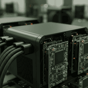
Level 1: Continuous sensor monitoring. Every production run generates hundreds of sensor traces — temperature profiles, RF power/impedance, gas flow rates, chamber pressure, endpoint signals. AI models trained on historical sensor data from well-matched chambers establish a baseline “sensor fingerprint” for each chamber. Deviations from this fingerprint are detected within seconds, not weeks. The system processes over 500 sensor parameters per chamber per process step, far beyond what any human engineer can monitor simultaneously.
Level 2: Virtual matching assessment. Using Virtual Metrology models, the system predicts what the wafer output metrics (thickness, uniformity, defect density) would be for each chamber based on the current sensor data — without processing a golden wafer. This virtual matching assessment runs continuously, providing an always-current matching status for every chamber. Field deployments show that virtual matching assessments correlate with physical golden wafer measurements at R-squared values above 0.93.
Level 3: Root cause diagnosis and corrective recommendations. When the system detects a matching drift, it does not simply flag an alarm. It identifies the specific sensor parameters that have shifted, correlates them with known physical mechanisms (e.g., “RF impedance drift in chamber 3 consistent with quartz window coating buildup”), and recommends specific corrective actions with predicted effectiveness. This diagnostic capability reduces the time from drift detection to corrective action from days to hours.
What Results Does AI Chamber Matching Deliver?
Field data from MST’s NeuroBox deployments across CVD, etch, and PVD processes demonstrates consistent improvements:
Yield impact. Matching-related yield loss reduced by 25-40% compared to golden wafer-only matching. The improvement comes primarily from catching drift events between scheduled matching intervals — events that previously went undetected until downstream metrology or yield analysis.
Golden wafer elimination. Production sites using AI chamber matching have reduced golden wafer consumption by 70-90%. Some sites have moved to a validation-only model where golden wafers are run quarterly as a regulatory compliance check rather than as the primary matching method.
Engineering efficiency. Process engineer time spent on matching activities decreased by 50-60%. The AI system handles routine monitoring and diagnosis; engineers focus on complex multi-variable drift events and new process development.
Scheduling flexibility. With continuous matching status visibility, production scheduling systems can route wafers to any well-matched chamber with confidence. Chamber utilization balance improved by 12-18% in deployments where AI matching data was integrated with the manufacturing execution system (MES).
How Does AI Handle Multi-Tool, Multi-Chamber Complexity?
The complexity of chamber matching scales non-linearly. Matching 4 chambers on one tool requires 6 pairwise comparisons. Matching 12 chambers across 3 tools requires 66 pairwise comparisons. Matching 48 chambers across 12 tools — common for high-volume processes — requires 1,128 pairwise comparisons. At this scale, manual matching management becomes physically impossible.
AI excels at exactly this type of high-dimensional monitoring. MST’s NeuroBox system maintains a matching matrix that is updated in real time for every chamber-to-chamber pair. The matrix visualization provides fab engineers with an instant overview of fleet-wide matching status — green for well-matched pairs, yellow for drifting pairs, red for out-of-specification pairs.
The system also identifies correlated drift patterns — situations where multiple chambers drift in the same direction simultaneously, indicating a shared root cause such as a facility gas supply change or a cleanroom temperature shift. These fleet-wide patterns are invisible to per-chamber analysis but obvious to an AI system monitoring all chambers simultaneously.
Why Is Now the Right Time to Transition?
Three converging trends make AI chamber matching a strategic priority in 2026-2027:
Advanced node requirements. At 3nm and below, process windows are measured in fractions of nanometers. The tolerance for chamber-to-chamber variation that was acceptable at 28nm is physically incompatible with advanced node requirements. AI’s ability to detect sub-angstrom drift patterns is not a luxury — it is a manufacturing requirement.
Fab expansion economics. With $530 billion in new fab construction underway globally, the number of chambers requiring matching management is increasing dramatically. Companies building matching infrastructure on AI foundations today will scale efficiently; those relying on golden wafer methods will face engineering headcount requirements that grow linearly with chamber count.
Data infrastructure maturity. The sensor data required for AI chamber matching has always existed — equipment generates it during every production run. What has changed is the availability of edge computing hardware capable of processing this data in real time (NeuroBox), and the maturity of ML models specifically designed for semiconductor process data. The technical barriers have been removed; the remaining barrier is organizational willingness to adopt a new approach.
Chamber matching is not a glamorous topic. It does not generate headlines or attract venture capital attention. But for the engineers and managers who run semiconductor production lines, it is one of the most impactful applications of AI in the fab — a direct, measurable improvement in yield, efficiency, and operational control that pays for itself within months of deployment.
Deploy real-time AI process control with sub-50ms latency on your production line.