- →Why Is Wafer Inspection Becoming the Data Bottleneck of Advanced Fabs?
- →What Are the Key Defect Types and Why Are They Hard to Classify?
- →How Does AI Revolutionize Defect Detection and Classification?
- →How Does AI Reduce the Defect Review Bottleneck?
- →How Is AI Deployed for Wafer Inspection Intelligence?
Key Takeaway
Wafer defect inspection generates terabytes of image data daily, yet 30-50% of detected defects are nuisance defects that waste engineering time, and true killer defects are often misclassified or buried in noise. AI-powered automated defect recognition (ADR) and classification (ADC) can process inspection images 100x faster than human operators, achieve classification accuracy above 95% across 50+ defect types, and reduce the defect review bottleneck from hours to minutes — enabling fabs to find killer defects earlier, classify them accurately, and trace them to root causes in real time.
Why Is Wafer Inspection Becoming the Data Bottleneck of Advanced Fabs?
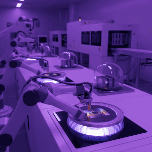
Wafer inspection is the eyes of the semiconductor fab — without it, process engineers are blind to the defects that kill yield. A modern logic fab performs 30-50 inspection steps per wafer flow, using a combination of optical inspection (brightfield and darkfield), e-beam inspection, and review SEM. Each inspection step generates enormous amounts of data: a single KLA 3900 series broadband plasma inspection of a 300mm wafer detects 10,000-500,000 defect events, each with associated coordinates, signal strength, and thumbnail images.
The data volume is staggering. A 50,000 wafer-per-month fab running 40 inspection steps per flow generates 2-20 billion defect events per month. Even with aggressive filtering (removing repeater defects, design-systematic defects, and known nuisance sources), the remaining population of 50-200 million defects per month must be classified and analyzed to drive yield improvement.
The traditional approach to defect classification relies on two sequential steps:
Automatic Defect Classification (ADC): Rule-based algorithms classify defects into 10-30 categories based on signal characteristics (size, brightness, shape, location relative to pattern). Current rule-based ADC achieves 60-80% classification accuracy, with the remaining 20-40% either misclassified or assigned to a “catch-all” unclassified bin.
Manual Defect Review (MDR): Human operators review SEM images of sampled defects, visually classifying them into 30-100 detailed defect types. A skilled operator can classify 100-200 defects per hour. With 10,000-50,000 defects requiring review per day, the manual review bottleneck limits the speed of yield learning.
The cost of this bottleneck is enormous. Yield engineers estimate that 50-70% of their time is spent on defect data management — collecting, classifying, filtering, and analyzing defect data — rather than on actual root-cause identification and process improvement. Faster, more accurate defect classification directly accelerates the yield learning rate, which determines how quickly a fab reaches profitable yield on new process nodes.
What Are the Key Defect Types and Why Are They Hard to Classify?
Semiconductor defects span a wide taxonomy that evolves with each technology node:
Particle defects: Foreign material on the wafer surface, ranging from 20nm to several micrometers. Sources include equipment wear (robot arm particles, chamber flaking), chemical contamination (slurry residue from CMP, undissolved particles in chemicals), and cleanroom environment (airborne particles, human-generated contamination). Particles are relatively easy to detect but difficult to trace to source because they originate from diverse equipment and processes.
Pattern defects: Deviations in the printed pattern, including line breaks (opens), line bridges (shorts), missing features, extra features, and pattern displacement. These are typically caused by lithography or etch process issues. At sub-7nm nodes, the distinction between a “real” pattern defect and a normal process variation becomes increasingly ambiguous, requiring SEM review at 50,000-200,000x magnification.
Film defects: Voids in deposited films, delamination between layers, surface roughness anomalies, and crystallographic defects. These are often subsurface and detectable only by specific inspection modes (e.g., darkfield inspection at oblique illumination angles).
Scratch and handling defects: Mechanical damage from wafer handling, cassette contact, and CMP processing. These defects are typically elongated and follow specific directional patterns that distinguish them from other defect types.
Electrical defects: Visible only through e-beam inspection (voltage contrast), these defects appear as bright or dark contacts/vias indicating open or resistive connections that would not be visible in optical inspection.
The classification challenge increases at advanced nodes because: (1) defect sizes approach the optical resolution limit, making shape analysis unreliable; (2) the number of distinct defect types increases (from 20-30 at 28nm to 50-100+ at 3nm); (3) nuisance defect rates increase as inspection sensitivity is pushed to detect smaller real defects; and (4) pattern complexity makes it harder to distinguish defects from intentional design features.
How Does AI Revolutionize Defect Detection and Classification?
AI-powered defect inspection uses deep learning — specifically Convolutional Neural Networks (CNNs) and more recently Vision Transformers — to classify defects from inspection images with accuracy that matches or exceeds human experts:
Image-based classification: The AI model processes the SEM review image (or high-resolution optical inspection image) of each defect and classifies it into one of 50-100+ defect categories. Modern architectures achieve greater than 95% classification accuracy across all categories, compared to 60-80% for rule-based ADC and 90-95% for experienced human operators.
Multi-modal fusion: The most advanced systems combine multiple data sources for each defect: the optical inspection signal (including multiple illumination modes), the SEM review image, the design layout at the defect location (to understand what pattern should be there), and the process history of the wafer (to provide context about which defect types are likely). This multi-modal approach improves classification accuracy by 5-10% over image-only models.
Nuisance filtering: AI models learn to distinguish true defects from process-inherent noise and design-related signals. By training on labeled examples of nuisance defects, the model can filter 80-90% of nuisance events with less than 0.1% loss of real defects. This is critical because nuisance defects can outnumber real defects by 10-100x at high inspection sensitivity.
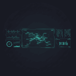
Defect clustering and source analysis: Beyond individual defect classification, AI algorithms analyze the spatial distribution of defects across the wafer and across lots to identify systematic patterns. Radial patterns suggest CMP or spin-coat issues; concentric arc patterns suggest wafer handling or edge contact; field-periodic patterns suggest lithography or reticle problems. AI pattern recognition identifies these spatial signatures automatically, dramatically accelerating root-cause analysis.
Small-sample learning: A key practical challenge is that new defect types emerge as processes change, and initially there are very few examples for training. Modern few-shot learning techniques enable the AI model to learn a new defect class from as few as 10-20 labeled examples, compared to the hundreds or thousands typically needed for traditional deep learning. This allows the system to adapt to new defect modes within hours rather than weeks.
How Does AI Reduce the Defect Review Bottleneck?
The defect review SEM (DRSEM) is one of the most expensive bottlenecks in the fab. A single review SEM costs $3M-$5M, operates at 100-200 defects per hour for thorough review, and a typical fab needs 5-15 review SEMs to handle the defect volume. AI reduces this bottleneck through several mechanisms:
Intelligent sampling: Instead of randomly sampling defects for review, the AI system identifies which defects are most informative — new defect types not previously seen, defects at unusual locations, and defects that the classifier has low confidence on. This targeted sampling extracts maximum information from each reviewed defect, reducing the total review volume by 50-70% while maintaining or improving yield learning speed.
Virtual review: For defect types that the AI classifier handles with high confidence (greater than 98%), the SEM review step can be skipped entirely. The AI classification from the inspection tool’s optical image is sufficient for yield analysis. This eliminates review for 40-60% of all defect events, freeing review SEM capacity for the defects that truly need high-resolution imaging.
Automated root-cause linkage: The AI system correlates classified defects with equipment trace data, maintenance logs, and chemical batch records to automatically suggest root causes. When the system detects a spike in particle defects of a specific type, it can immediately narrow the suspect list to 2-3 most likely equipment sources based on historical correlation — a task that traditionally took a yield engineer several hours of manual analysis.
Real-time yield impact estimation: Not all defects are equally harmful. The AI system estimates the probability that each defect is a “killer defect” based on its type, size, location relative to active device areas, and the specific device design. This kill probability estimation enables prioritized response — focusing engineering attention on the defects that actually limit yield rather than on the most numerous defects (which are often the least harmful).
How Is AI Deployed for Wafer Inspection Intelligence?
The NeuroBox E5200V platform is specifically designed for visual inspection and defect intelligence in semiconductor manufacturing:
Edge inference for real-time classification: The E5200V’s GPU-accelerated edge computing processes inspection images in real time, classifying each defect as the inspection tool operates. This eliminates the offline batch processing that typically delays defect classification by 2-6 hours after inspection.
Integration with inspection ecosystem: The system interfaces with major inspection platforms (KLA broadband plasma, Onto Innovation USIS, Applied Materials SEMVision) through standard data formats (KLARF, SEMI E142). This allows deployment alongside existing inspection tools without requiring changes to the inspection hardware or recipes.
Continuous model improvement: When engineers correct a classification during manual review, the feedback is automatically incorporated into the model through incremental learning. Over weeks and months, the model progressively improves as it learns from the specific defect population of each fab, process, and technology node.
Cross-layer defect correlation: The system tracks defects across multiple inspection layers, identifying which inline defects predict final test failures. This multi-layer correlation is critical for determining which inspection steps are truly yield-relevant and which can be relaxed to save inspection capacity.
For process development and new technology node bring-up, the E5200V’s automated defect classification accelerates the yield learning rate by 2-3x compared to manual classification. In the critical first 6 months of a new node’s production ramp, this acceleration can be worth tens of millions of dollars in earlier achievement of profitable yield.
What Business Impact Does AI Deliver for Wafer Inspection?
The ROI for AI-powered defect inspection spans capital efficiency, operational efficiency, and yield improvement:
Review SEM capacity savings: Reducing DRSEM workload by 50-70% through intelligent sampling and virtual review effectively eliminates the need for 2-5 review SEMs ($6M-$25M in avoided capital). Additionally, the labor cost of 10-20 defect review operators ($500K-$1M annually) is largely eliminated.
Faster yield learning: Accelerating defect classification from hours to minutes means yield engineers can respond to excursions within the same shift rather than the next day. Industry data suggests that fabs with real-time defect intelligence achieve target yield 2-4 months earlier on new technology nodes. At $20M-$50M in monthly wafer revenue at production yield, each month of acceleration is directly valuable.
Reduced nuisance defect overhead: Eliminating 80-90% of nuisance defects from the analysis pipeline saves 3-5 hours of yield engineering time per day — time that can be redirected to actual process improvement. Across a team of 10-20 yield engineers, this is equivalent to adding 2-4 FTEs without hiring.
Improved excursion response: AI-powered real-time defect monitoring detects process excursions within 1-2 lots (compared to 5-10 lots with traditional daily defect review), reducing excursion-related scrap by 60-80%. For a fab with 0.5-1% excursion-related scrap rate, this improvement is worth $3M-$6M annually.
Inspection recipe optimization: By understanding which defect types actually impact yield (through kill probability estimation), fabs can optimize inspection sensitivity for each step — increasing sensitivity for yield-critical steps and relaxing it for less critical steps. This rebalancing improves overall defect capture while maintaining or increasing inspection throughput.
Total annual value for a medium to large fab: $10M-$30M against a NeuroBox E5200V deployment investment of $500K-$1.5M. The combination of capital avoidance, labor savings, faster yield ramp, and reduced scrap makes defect inspection AI one of the most broadly impactful applications in the semiconductor manufacturing intelligence portfolio.
Deploy real-time AI process control with sub-50ms latency on your production line.