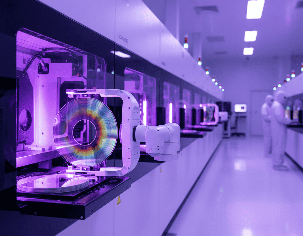
- →Why Is Lithography the Most Metrology-Intensive Process in the Fab?
- →What Causes Overlay and CD Errors in Modern Lithography?
- →How Can AI Predict Overlay Before Measurement?
- →How Does AI Optimize Exposure Dose and Focus?
- →How Is AI Deployed in the Lithography Module?
Key Takeaway
Lithography overlay and CD control consume up to 40% of a modern fab’s metrology capacity, yet excursions still slip through sampling gaps. AI models that combine scanner lens signatures, reticle heating profiles, wafer chuck temperature maps, and inline alignment data can predict overlay errors within 0.3nm and optimize exposure dose lot-by-lot — reducing overlay excursions by 60% and cutting rework rates from 3-5% to below 1% at advanced EUV nodes.
Why Is Lithography the Most Metrology-Intensive Process in the Fab?
Lithography defines every pattern on a semiconductor device, making it the single most yield-critical process in the fab. At the 3nm node using EUV (Extreme Ultraviolet) lithography, the overlay specification — the alignment accuracy between consecutive patterning layers — is typically 1.5-2.0nm. To put that in perspective, this is roughly 7-10 silicon atoms. A single nanometer of overlay error can cause contact-to-gate shorts, via misalignment, or interconnect opens that kill entire die.
The metrology burden is enormous. A typical advanced logic fab dedicates 35-45% of its total metrology capacity to lithography, including overlay measurement, CD-SEM for pattern fidelity, and scatterometry for resist profile. Each lot requires 15-25 minutes of metrology time per layer per tool, and with 60-80 critical lithography layers in a modern device, the metrology bottleneck directly limits fab throughput.
Despite this massive measurement investment, the sampling rate remains painfully low. Overlay is typically measured on 15-30 sites per wafer on 3-5 wafers per lot. This means less than 0.1% of all die locations are actually measured — the rest are inferred through statistical models. When a systematic error pattern changes between sampled wafers, the excursion goes undetected until yield loss appears at final test, days or weeks later.
What Causes Overlay and CD Errors in Modern Lithography?
Overlay errors arise from the interaction of multiple error sources that vary on different timescales:
Scanner-related errors: Lens aberrations, stage positioning accuracy (controlled to sub-nanometer level by interferometry), reticle stage drift, and illumination non-uniformity. Modern ASML NXE:3600 EUV scanners have 50+ adjustable lens elements (manipulators) that compensate for aberrations, but optimal settings drift with thermal loading and component aging.
Reticle-related errors: Pattern placement errors on the mask (0.5-1.5nm at wafer level after 4x reduction), reticle heating during exposure causing image distortion (up to 0.8nm at high dose), and pellicle-induced wavefront errors for DUV layers.
Wafer-related errors: Film stress-induced wafer distortion (bow and warp changes of 10-50 micrometers after high-temperature processing), CMP-induced thickness variations affecting focus, and prior-layer pattern placement errors that accumulate through the process flow.
Process-related errors: Resist thickness non-uniformity affecting CD through swing curve effects, post-exposure bake temperature non-uniformity causing CD variation of 0.5-1.5nm per degree Celsius, and develop process variations.
CD control faces an equally complex challenge. The target CD is typically controlled through exposure dose (measured in mJ/cm2) and focus. The dose-to-size sensitivity is 2-5nm per percent dose change, meaning even 0.5% dose variation causes measurable CD shift. Focus errors create asymmetric profiles and increase CD variation through the depth of focus — a particular concern for EUV with its inherently shallower depth of focus compared to DUV.
How Can AI Predict Overlay Before Measurement?
AI-powered overlay prediction works by learning the complex relationships between upstream process data and downstream overlay errors. The model inputs include:
Scanner sensor data: Wafer alignment measurements (typically 20-40 alignment marks measured per wafer during loading), lens heating model outputs, stage positioning telemetry, focus-leveling sensor data across the exposure field, and dose uniformity monitor readings. Modern scanners output 500-2,000 data points per wafer from these sensors.
Process history data: The complete processing history of each wafer including film deposition conditions, anneal temperatures, CMP removal amounts, and prior lithography overlay corrections. This contextual data captures the wafer-induced overlay components that the scanner cannot directly measure.
Environmental data: Cleanroom temperature and humidity variations (which affect resist properties and scanner optics), barometric pressure changes (which shift scanner interferometer readings), and vibration monitoring data.
The AI model — typically an ensemble of gradient-boosted trees for tabular features and convolutional networks for spatial wafer maps — learns to predict the full-wafer overlay map (typically on a 13×13 grid per field, across all fields) from these inputs. The prediction is available within seconds of exposure completion, compared to the 15-25 minute wait for physical metrology.
Key accuracy metrics from production deployments: overlay prediction MAE of 0.2-0.4nm (compared to the metrology tool repeatability of 0.1-0.2nm), with a correlation coefficient above 0.90 between predicted and measured overlay across all wafer locations.
How Does AI Optimize Exposure Dose and Focus?
Beyond overlay prediction, AI enables intelligent dose and focus optimization that goes far beyond traditional lot-to-lot corrections:
Wafer-level dose optimization: By combining virtual metrology predictions of incoming film thickness (from CVD/PVD AI models) with the known dose-to-size relationship, the system calculates the optimal dose for each lot — and potentially each wafer — before it reaches the scanner. This feedforward path reduces CD lot-to-lot variation by 20-30%.
Intra-field dose and focus correction: Modern scanners support field-by-field and even intra-field dose and focus adjustments. AI models that predict the expected CD variation pattern across the field (based on reticle error, lens signature, and resist process data) can compute optimal intra-field corrections that reduce within-field CD range by 15-25%.
Thermal dose compensation: During high-volume scanning, reticle heating causes progressive image distortion. The AI model tracks the reticle thermal state based on exposure history and ambient conditions, predicting the distortion 3-5 fields ahead and pre-compensating through scanner adjustments. This eliminates the first-wafer effect that typically causes the first 2-3 wafers of each lot to have 0.5-1nm worse overlay.
Multi-layer co-optimization: Rather than optimizing each lithography layer independently, the AI system considers the cumulative overlay budget across all layers and allocates correction capability where it has the most impact on yield. This systems-level optimization typically improves the overall overlay performance by 10-15% compared to layer-by-layer optimization.
How Is AI Deployed in the Lithography Module?
The NeuroBox E3200 platform interfaces with the lithography ecosystem through multiple data paths:
Scanner integration: Data is collected from the scanner host computer via SECS/GEM and from the scanner’s advanced process control (APC) interface. This includes all alignment, leveling, and correction data for every wafer. The latency requirement is strict — overlay correction updates must be available within 30 seconds of the previous wafer’s exposure to be applicable to the next wafer in the lot.
Track integration: Resist coat and develop process data (spin speed, bake temperatures, develop time and temperature) feeds into the CD prediction model. Track equipment from TEL and SCREEN generates 30-80 sensor channels per wafer, providing rich input for resist process state estimation.
Metrology feedback loop: When physical overlay or CD measurements are available (typically 3-5 wafers per lot), the AI model updates its predictions and recalibrates. The system uses a Bayesian updating framework that smoothly blends model predictions with measurements, weighted by their respective uncertainties.
APC integration: The AI system’s overlay and CD predictions feed into the existing APC system (such as KLA LithoStar or ASML BaseLiner) as virtual metrology inputs. This allows the APC system to compute corrections on every wafer rather than only on measured wafers, dramatically improving the effective control bandwidth.
For new process development and qualification scenarios, the NeuroBox E5200 supports Smart DOE for lithography process window optimization. By intelligently exploring the dose-focus-overlay parameter space, the system identifies the optimal process window with 60-75% fewer test wafers than traditional focus-exposure matrix methods.
What Business Value Does AI Deliver for Lithography?
Lithography is the highest-value target for AI in the fab, with returns that justify significant investment:
Overlay excursion reduction: AI-powered prediction with 100% virtual inspection reduces overlay excursions by 55-65% compared to traditional sampled inspection. For a fab where overlay excursions cause 0.5-1% scrap rate, this translates to $7M-$15M in annual savings.
Rework reduction: Lithography rework (stripping and re-exposing out-of-spec wafers) costs $200-$500 per wafer and adds 8-24 hours of cycle time. Reducing the rework rate from 3-5% to below 1% through better feed-forward control saves $3M-$8M annually for a 50,000 wafer-per-month fab.
Metrology capacity release: By replacing 60-80% of physical overlay measurements with high-confidence virtual metrology, the fab frees up $5M-$10M worth of metrology tool capacity that can be redeployed to support new process development or increase production throughput.
Scanner productivity improvement: Faster lot setup through AI-predicted correction recipes (versus waiting for measurement-based corrections) improves effective scanner utilization by 2-4%. Given that a single EUV scanner costs $150M-$200M and processes 1,500-2,000 wafers per day, even a 2% productivity improvement is worth $5M-$10M annually per scanner.
The combined annual value for a lithography module with 5-10 scanners ranges from $20M to $40M against a deployment investment of $500K-$1M. This makes lithography AI arguably the single highest-ROI application in the entire semiconductor manufacturing value chain.
Deploy real-time AI process control with sub-50ms latency on your production line.