- →Why Does Thin Film Uniformity Matter So Much at Advanced Nodes?
- →What Makes CVD and PVD Process Control Particularly Challenging?
- →What Real-Time Sensor Data Is Available for AI Modeling?
- →How Do AI Models Predict Film Thickness and Uniformity?
- →How Does AI Enable Closed-Loop Deposition Control?
Key Takeaway
CVD and PVD thin film deposition are among the most sensor-rich processes in semiconductor manufacturing, yet thickness and uniformity control still relies heavily on post-deposition metrology with 30-60 minute feedback delays. AI models processing real-time chamber sensor data — including RF power, gas flow, temperature, and optical emission — can predict film thickness within 0.5% accuracy and within-wafer uniformity within 0.2%, enabling wafer-to-wafer recipe adjustment that cuts thickness variation by 35-50%.
Why Does Thin Film Uniformity Matter So Much at Advanced Nodes?
Every semiconductor device is built layer by layer through hundreds of thin film deposition steps. Chemical Vapor Deposition (CVD) and Physical Vapor Deposition (PVD) together account for 30-40% of all process steps in a modern logic or memory fab. At the 3nm node, a typical device stack requires over 100 distinct deposition steps producing films ranging from sub-nanometer atomic layer deposition (ALD) barriers to multi-micrometer thick interlayer dielectrics.
The uniformity requirements are staggering. For a high-k gate dielectric at 2nm equivalent oxide thickness, the uniformity specification is typically plus or minus 0.5 angstrom (2.5%) across a 300mm wafer — roughly one atomic layer. For copper seed layers in dual-damascene metallization, the thickness uniformity directly impacts electromigration reliability and via resistance distribution.
The financial impact of deposition non-uniformity compounds through the process flow. A 1% thickness non-uniformity in a CVD oxide film translates to a 1-3% CD variation after the subsequent etch step (due to etch rate dependence on film properties), which in turn causes 0.5-1% yield loss at final test. For a high-volume fab producing 50,000 wafers per month, each percentage point of yield is worth $20M-$30M annually.
What Makes CVD and PVD Process Control Particularly Challenging?
CVD processes deposit films through chemical reactions of precursor gases on the heated wafer surface. The deposition rate depends on precursor flow rates (typically measured in sccm with 0.1% resolution), chamber pressure (0.1-10 Torr), wafer temperature (200-800 degrees Celsius depending on the process), RF power for plasma-enhanced CVD (100-2000W), and the state of chamber wall deposits that accumulate over 500-2000 wafers between cleans.
PVD (sputtering) deposits films by bombarding a target material with argon ions, ejecting atoms that land on the wafer. Key variables include DC or RF power (1-20 kW), argon pressure (1-10 mTorr), target-to-wafer distance, magnet configuration, and target erosion profile that changes with usage.
The dominant control challenge for both CVD and PVD is chamber conditioning drift. After a wet clean, the chamber walls are bare — no deposits — creating a fundamentally different chemical environment than a seasoned chamber. The first 100-300 wafers after cleaning show measurable drift in deposition rate (typically 2-5% decrease as walls season) and film properties. Traditional control uses conservative fixed seasoning recipes, often wasting 50-100 production wafers in qualification.
Additionally, consumable degradation creates long-term drift. A PVD target loses 30-50% of its material over its lifetime (5,000-15,000 kWh), and the erosion profile changes the sputtering geometry, shifting the uniformity pattern from center-thick to edge-thick. CVD showerhead hole clogging or precursor line degradation causes similar systematic shifts.
What Real-Time Sensor Data Is Available for AI Modeling?
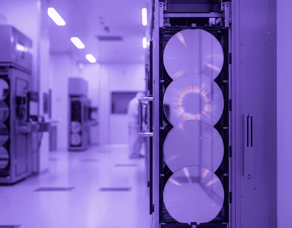
Modern CVD and PVD tools are among the most heavily instrumented equipment in the fab. A single AMAT Endura PVD or Lam Vector PECVD chamber generates 80-300 sensor channels, providing rich input features for AI models:
Thermal sensors: Multi-zone heater power and temperature (typically 5-15 zones for CVD, providing a direct proxy for the temperature profile across the wafer), chamber wall thermocouples, showerhead temperature, and exhaust gas temperature.
Gas and pressure sensors: Mass flow controllers (MFC) with actual vs. setpoint readings for each gas line (revealing MFC drift), chamber pressure via capacitance manometer, throttle valve position, and foreline pressure.
Plasma sensors (for PECVD/PVD): RF forward and reflected power, DC bias voltage (self-bias), plasma impedance, and optical emission spectroscopy for plasma composition monitoring.
Mechanical sensors: Susceptor position, wafer rotation speed, shutter position and timing, robot arm alignment data, and gas line pressures upstream of MFCs.
In-situ optical monitoring: Some advanced CVD tools include in-situ ellipsometry or reflectometry that can measure film thickness during deposition. However, these are expensive, require optical access ports, and are limited to optically transparent films.
The data volume is substantial: a single CVD chamber processing 500 wafers per day generates 1-3 GB of sensor data daily. Across a typical CVD/PVD bay of 20-40 chambers, the total data volume reaches 20-120 GB per day — far beyond what human engineers can analyze manually.
How Do AI Models Predict Film Thickness and Uniformity?
The AI approach to CVD/PVD virtual metrology uses the full sensor time-series from each deposition run to predict the resulting film thickness, uniformity, and key film properties (stress, refractive index, resistivity). The modeling pipeline includes several key innovations:
Feature engineering from physics: Rather than blindly feeding raw sensor data into a model, the best approaches incorporate domain knowledge. For example, the integrated RF energy (power multiplied by time) is a strong first-order predictor of PVD film thickness. The ratio of heater power to susceptor temperature reveals thermal mass changes from wall buildup. Gas flow ratios (e.g., SiH4/N2O for SiO2 deposition) capture stoichiometry variations.
Multi-scale temporal modeling: Film deposition involves both fast dynamics (second-to-second plasma fluctuations) and slow dynamics (wafer-to-wafer chamber drift). The AI architecture uses parallel processing paths: convolutional layers capture within-wafer process signatures, while recurrent layers track chamber-state evolution across sequential wafers.
Transfer learning across chambers: A model trained on one chamber can be fine-tuned for a matched chamber using only 200-500 wafers of data, compared to the 3,000-5,000 wafers needed for training from scratch. This dramatically accelerates deployment across the fab. The NeuroBox E3200 platform supports this transfer learning workflow natively, maintaining a model registry that tracks the lineage and performance of each chamber-specific model.
Uncertainty quantification: Critical for production use, the model outputs a confidence interval alongside each prediction. When confidence drops below a threshold (typically due to a novel chamber state not seen during training), the system automatically flags the wafer for physical metrology, ensuring that the virtual metrology system fails safe.
Typical prediction accuracy: film thickness MAE of 0.3-0.8% for CVD oxide and nitride films, 0.5-1.2% for PVD metal films, and within-wafer uniformity prediction within 0.15-0.3% (1 sigma).
How Does AI Enable Closed-Loop Deposition Control?
The real power of AI virtual metrology emerges when predictions feed back into process control. The NeuroBox E3200 implements this through a three-tier control architecture:
Tier 1 — Run-to-Run (R2R) control: After each wafer, the virtual metrology prediction updates a Kalman filter that tracks the chamber state. The controller adjusts deposition time, temperature setpoint, or RF power for the next wafer to compensate for drift. This loop runs autonomously with no human intervention, maintaining thickness within specification even as chamber conditions slowly change.
Tier 2 — Lot-to-lot feedforward: When incoming wafer metrology (from a prior process step) is available, the controller adjusts the recipe proactively. For example, if the pre-deposition oxide thickness is 2% thinner than target, the CVD recipe can add 2% more film to compensate. This feedforward path reduces the total stack thickness variation by 20-30% beyond what feedback alone can achieve.
Tier 3 — Preventive maintenance optimization: By tracking the trajectory of chamber drift, the AI system predicts when the chamber will exit the controllable window and require a wet clean or consumable replacement. This converts maintenance from calendar-based scheduling to condition-based scheduling, extending chamber uptime by 5-15% while preventing quality excursions.
In production deployment at a major DRAM manufacturer, the three-tier AI control system reduced PECVD silicon nitride thickness variation (wafer-to-wafer, 1 sigma) from 1.2% to 0.6% — a 50% improvement. The within-wafer uniformity improved from 1.8% to 1.1%. These improvements propagated through downstream etch and CMP steps, contributing to a cumulative yield improvement of 0.8% at die sort.
What Is the Deployment Roadmap and Expected ROI?
Deploying AI for CVD/PVD control follows a phased approach that delivers value at each stage:
Phase 1 (Months 1-2): Data collection and model training. Connect NeuroBox E3200 to target chambers, collect sensor data matched with metrology results. Minimum data requirement: 2,000-3,000 wafers per chamber per recipe. Cost: hardware plus integration, approximately $120K-$180K per chamber.
Phase 2 (Months 3-4): Virtual metrology deployment. Deploy trained models for real-time thickness prediction. Engineers use the predictions for monitoring and gain confidence in model accuracy. Typical accuracy: 95-98% of predictions within metrology tool specification. Immediate value: metrology sampling reduction by 3-5x, freeing $200K-$400K in metrology tool capacity annually.
Phase 3 (Months 5-6): Closed-loop R2R control. Enable automatic recipe adjustment based on virtual metrology. This is the highest-value phase, delivering $500K-$1.5M annually per chamber group in reduced scrap, improved yield, and extended maintenance intervals.
Phase 4 (Ongoing): Expansion and optimization. Roll out to additional chambers using transfer learning (2-4 weeks per new chamber versus 2 months for initial deployment). Integrate feedforward from upstream processes for full-stack thickness optimization.
For a typical deposition bay of 20 chambers, the fully deployed system delivers $3M-$8M in annual savings against a total investment of $400K-$600K (hardware, software, integration) — a payback period of less than 3 months and an ongoing ROI exceeding 500%. The key is starting with the highest-value chambers (typically the most drift-prone or yield-critical deposition steps) and expanding systematically based on demonstrated results.
Deploy real-time AI process control with sub-50ms latency on your production line.